Welcome: Shenzhen Zhuolida Electronics Co.TD
Language:
 ∷
∷

∷
∷
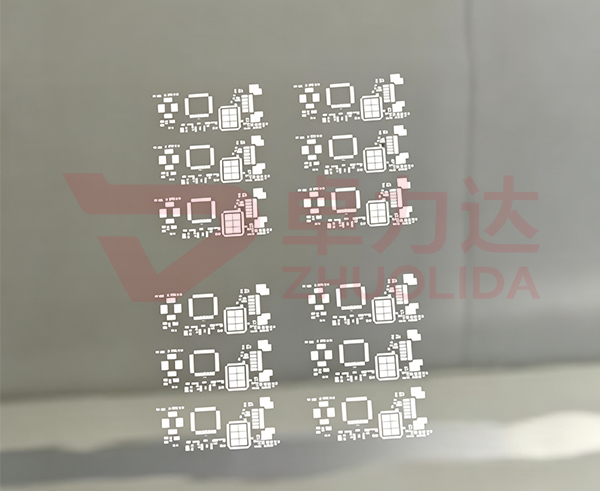
Ball shift, stencil deformation and uneven solder deposition are three common sources of yield loss on GPU packaging lines, and the problem usually lies not in the solder paste or placement equipment but in the aperture accuracy and dimensional stability of the stencil itself. As the core tooling for large-format FC-BGA ball placement, solder paste printing and micro-bump positioning, the GPU chip electroformed stencil directly determines packaging yield and signal reliability through its aperture tolerance, hole-wall finish and tension. This article walks through the micron-level Precision Electroforming process and breaks down the key parameters and selection criteria. For advanced packages such as large-format GPUs and HBM stacking, stencil quality directly determines first-pass yield and rework cost.
Compared with conventional laser cutting, GPU chip electroformed stencil manufacturing typically forms the stencil in one piece by pulsed precision electroforming: the process starts with high-precision film or LDI exposure to reproduce the micron-level aperture layout, followed by layer-by-layer electrochemical deposition of nickel-cobalt alloy; stress relief, tension calibration and dimensional setting are then carried out to avoid deformation during high-temperature printing; finally, full-size inspection, hole-wall polishing and registration verification are performed before the stencil leaves the factory, matched to the packaging equipment parameters.
In terms of measured parameters, the GPU chip electroformed stencil achieves an aperture accuracy of ±1–2 μm, supporting ultra-fine bump pitches of 40 μm and below; hole-wall roughness is controlled within Ra 0.6 μm for uniform solder paste release, reducing peaks, insufficient solder and cold joints. The stencil is made of high-toughness nickel-cobalt alloy, which is heat-resistant, fatigue-resistant and resistant to deformation, so apertures do not shift or collapse during long-run printing.
Tension stability is a hidden indicator in mass production. The finished GPU chip electroformed stencil is normally tensioned to 38–45 N/cm, remaining uniform across the large frame, ensuring accurate, drift-free registration during prolonged high-speed printing. As for service life, the electroformed one-piece construction has no splice seams and delivers excellent consistency across high-density apertures, with wear resistance and durability clearly superior to conventional laser-cut stencils, making it better suited to continuous high-volume GPU printing.
Take a typical large-format FC-BGA package as an example: a laser-cut stencil tends to develop rough hole walls and poor release in fine-pitch areas, causing repeated skips and bridging. After switching to a precision electroformed stencil, solder deposition becomes uniform and release is smooth, with significantly improved ball height consistency. This shows that in ultra-fine-pitch, large-substrate applications, the manufacturing process of the stencil matters more than surface treatment.
Clogging is the most common failure mode in high-frequency printing. GPU chip electroformed stencil manufacturing uses mirror-polished hole walls and optional nano-coating to reduce solder paste residue adhesion and extend the cleaning cycle. For the two industry pain points of ultra-fine hole clogging and rapid wear under high-frequency printing, optimized nickel-cobalt alloy formulations combined with surface treatment can bring significant improvement, making batch-to-batch consistency more stable.
In terms of applications, the mainstream fields served by GPU chip electroformed stencil manufacturers are highly concentrated: large-format FC-BGA packaging for AI training and inference GPUs, 2.5D stacking of HBM memory, automotive ADAS chips and accelerator card packaging, while remaining compatible with ABF build-up substrates and fine-line narrow-pitch designs. The industry trend toward higher density, finer pitch and larger size is deepening the reliance of these applications on electroformed stencils.
Different scenarios impose different requirements on the stencil: HBM stacking emphasizes aperture consistency and long-term life, power and thermal regions focus on high-temperature resistance and fatigue resistance, and the large GPU die core is more sensitive to aperture accuracy and registration accuracy. GPU chip electroformed stencil manufacturers should customize the stencil according to substrate specifications, equipment models and solder paste types; stepped stencils and nano-coating options can further adapt to the process window.
When evaluating a GPU chip electroformed stencil supplier, focus on four points: whether it has both precision electroforming and precision etching capabilities; whether it is equipped with high-precision inspection instruments for micron-level aperture and concentric registration checks; whether it can provide measured data on aperture tolerance and hole-wall roughness; and whether it offers DFM manufacturability analysis and rapid prototyping. During an on-site audit, pay particular attention to outgoing inspection reports and process parameter records.
Rollout can be broken down into three steps. First, provide packaging drawings and process parameters so the manufacturer can evaluate aperture layout and clearance risks. Second, make samples and measure aperture accuracy, hole-wall roughness and tension. Third, carry the sample parameters into mass production and track printing life. GPU chip electroformed stencil manufacturers that commit to explicit parameters deserve to move to small-batch validation.
Looking at the trends, AI computing is pushing GPU chips toward higher I/O counts, finer pitch and larger die size, shifting the requirement for stencils from "printable" to "repeatable high precision". The GPU chip electroformed stencil, and the manufacturers that produce it, need simultaneous improvements in aperture accuracy, wear resistance and consistency to support volume production of advanced packages.
Whether for large-format FC-BGA, HBM stacking or 2.5D heterogeneous integration, GPU chip electroformed stencil manufacturing and GPU chip electroformed stencil manufacturers have both proven in practice that as long as apertures are accurate, hole walls are smooth, tension is stable and inspection is closed-loop, the electroformed stencil can consistently support high-yield delivery in high-density GPU packaging.
Contact:赖先生
Phone:+86 18938693450
Tel:0755-2708-8292
Email:yw9@zldsmt.com
Add:深圳市宝安区福永镇新和村福园一路华发工业园A3栋
 Zhuolida