Welcome: Shenzhen Zhuolida Electronics Co.TD
Language:
 ∷
∷

∷
∷
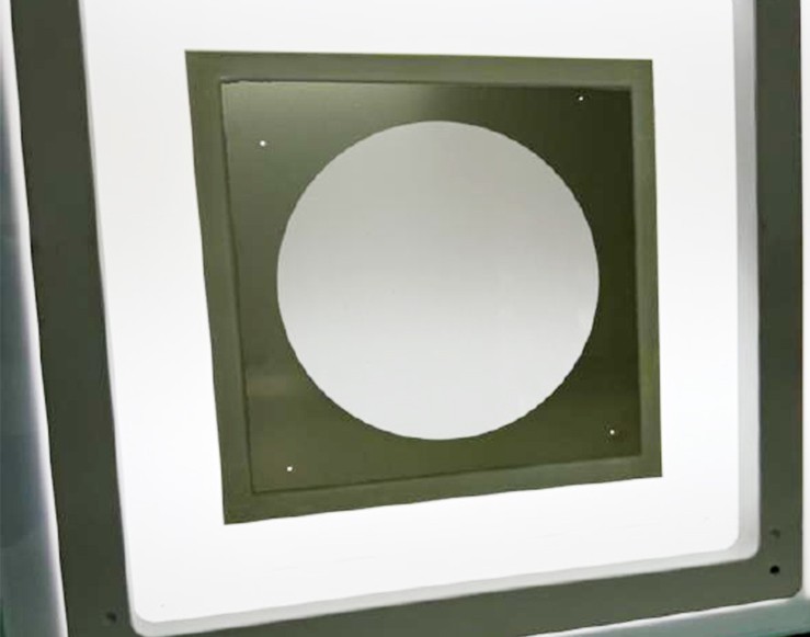
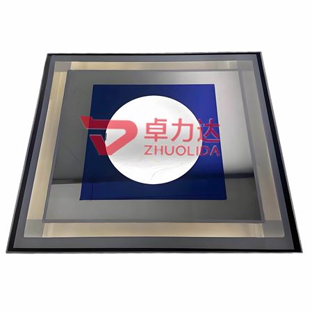
Wafer Electroforming Mask Processing is a specialized manufacturing technique that leverages metal electroforming to produce high-precision micro-nano patterned masks for semiconductor chip fabrication, packaging, and testing. Its core product, the wafer electroformed mask, serves as a critical supporting component in chip lithography and etching processes. This process combines photolithography masks with metal electroplating to precisely replicate complex patterns ranging from nanometer to micrometer scales. Compatible with mainstream wafer sizes like 8-inch and 12-inch wafers, it utilizes high-performance metals such as nickel and nickel-cobalt alloys. Key advantages include high pattern accuracy, absence of mechanical stress, and excellent dimensional consistency. The product enables high-density, fine-line pattern formation, effectively resolving issues such as pattern distortion and edge burrs common in traditional mask processing. It finds extensive application in semiconductor fields including IC chips, semiconductor sensors, and microelectromechanical systems (MEMS), providing core support for the miniaturization and high-precision production of chips.

Product Features
1. Nanoscale Precision Replication: Leveraging Precision Electroforming and deep ultraviolet lithography technology, it achieves accurate replication of micro-nano patterns with line widths ≤0.5μm. Line width tolerance is controlled within ±0.1μm, while pattern positioning accuracy reaches ±0.05μm—significantly surpassing traditional processing methods to meet the high-precision demands of advanced chip manufacturing.
2. Integrated Complex Pattern Formation: Supports one-step formation of intricate patterns including high-density structures, fine lines, and irregular apertures. Achieves pattern densities ≥1000 lines/mm without layered processing, effectively preventing misalignment from multi-layer stacking. Enhances mask stability and chip lithography precision.
3. Zero Mechanical Stress and Distortion: Utilizing a non-contact metal deposition process eliminates mechanical cutting and thermal influence zones, fully preserving material properties. This avoids residual stresses and pattern distortion inherent in traditional processing. Mask plate flatness is ≤0.01mm, ensuring precise pattern alignment with the wafer during lithography.
4. Strong Material Compatibility: Utilizes high-performance metals like nickel, nickel-cobalt alloys, and titanium alloys, offering superior corrosion resistance, wear resistance, and conductivity. Compatible with chemical environments in semiconductor manufacturing (e.g., photoresists, etching solutions), with no risk of material delamination or pattern damage during long-term use.
5. Superior Dimensional Consistency: Automated electroforming production lines and AI vision inspection systems provide real-time monitoring of critical parameters like pattern dimensions, line widths, and pitch. Mass-produced masks achieve dimensional consistency ≥99.8% and a yield rate of up to 99.7%, meeting semiconductor volume production demands.
6. Flexible Customization for Diverse Needs: Supports customization for mainstream wafer sizes including 8-inch and 12-inch. Custom masks with varying patterns, line widths, and thicknesses (0.05-0.2mm) can be produced based on customer chip design drawings. Suitable for manufacturing IC chips, MEMS, semiconductor sensors, and other products, with 24-hour rapid prototyping.
Product Performance
1. Precision Performance: Line width accuracy ±0.1μm, minimum line width down to 0.5μm, pattern positioning accuracy ±0.05μm, flatness ≤0.01mm, pattern edge roughness Ra≤0.05μm, free of burrs and serrations. Ensures precise replication of photolithography patterns, enhancing chip yield.
2. Mechanical Properties: When using nickel-cobalt alloy material, hardness reaches HV550+, tensile strength ≥600MPa. Withstands high-temperature and high-pressure environments during lithography without deformation or damage, with a service life exceeding 1000 lithography cycles.
3. Environmental Adaptability: Exceptional corrosion resistance withstands exposure to photoresists, etching solutions, and developers, passing corrosion tests exceeding 1000 hours. Operating temperature range spans -30°C to 120°C, adapting to semiconductor fabrication facilities' constant temperature and humidity environments with stable, non-degrading performance.
4. Pattern Performance: High pattern resolution enables high-density layout. Pattern transfer efficiency ≥99.9%. Post-lithography chip patterns exhibit no distortion or defects, effectively enhancing chip electrical performance and reliability.
5. Production Performance: Sample delivery within 24 hours; batch order lead time of 7-10 days. Fully automated production lines enable closed-loop control throughout the process. Metal ion recovery rate exceeds 90%, with energy consumption per unit reduced by 35% compared to traditional processing, balancing environmental sustainability and production efficiency.
6. Compatibility Performance: Compatible with mainstream lithography equipment and wafer sizes, supporting Deep Ultraviolet (DUV) and Extreme Ultraviolet (EUV) lithography systems. Adaptable to various photoresist types to meet diverse chip manufacturing process requirements.
Product Application Fields
1. IC Chip Manufacturing: Core application in the lithography stage for logic chips, memory chips, power chips, and other ICs. Serves as the core masking component for pattern transfer, precisely replicating chip circuit patterns to advance miniaturization and high-density development. Suitable for chip manufacturing in mobile phones, computers, servers, and other terminal devices.
2. Semiconductor Sensor Industry: Manufactures MEMS sensors, optoelectronic sensors, pressure sensors, and other semiconductor sensors. Through precise micro/nano pattern masks, it enables sensor miniaturization and high precision, serving smart wearables, automotive electronics, industrial control, and other applications.
3. Micro-Electro-Mechanical Systems (MEMS) Field: Supports manufacturing MEMS gyroscopes, MEMS accelerometers, and microfluidic chips. Leveraging complex pattern formation capabilities, it enables precision processing of MEMS device structures, enhancing sensitivity and stability.
4. Semiconductor Packaging: Processes lead frame and bump masks in chip packaging, precisely controlling pattern dimensions to enhance packaging accuracy and reliability. Supports mainstream packaging technologies including BGA, QFP, and CSP.
5. Optoelectronics: Used in manufacturing optoelectronic devices like optical communication chips, laser chips, and display panel driver chips. High-precision pattern masks enable accurate formation of optical paths and circuits, enhancing optoelectronic performance.
6. Other Semiconductor-Related Fields: Also applicable to processing semiconductor test fixtures, nanoimprint templates, and other products. Provides high-precision, high-reliability mask plate support services for upstream and downstream semiconductor supply chains, driving high-quality development in the semiconductor industry.
Contact:赖先生
Phone:+86 18938693450
Tel:0755-2708-8292
Email:yw9@zldsmt.com
Add:深圳市宝安区福永镇新和村福园一路华发工业园A3栋
 Zhuolida