Welcome: Shenzhen Zhuolida Electronics Co.TD
Language:
 ∷
∷

∷
∷
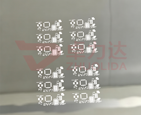
Benefiting from high density TSV through vias and short interconnection paths, 2.5D silicon interposers act as core carriers for heterogeneous integration of HBM and computing power Chiplet chips. As micro bump pitches keep shrinking and I/O array density rises sharply, ball placement and flux printing procedures impose stringent constraints on tooling. Conventional laser cut and etched templates suffer from aperture wall burrs, thermal stress deformation and side etching aperture enlargement. These defects readily trigger solder paste adhesion, bridging, micro bump missing printing and even scratches on brittle silicon surfaces, making them unfit for mass production conditions of silicon interposers. The 2.5D silicon interposer electroformed template adopts monolithic nickel cobalt alloy pulse electroforming. Free from mechanical cutting stress, it delivers high fidelity reproduction of micro aperture arrays and mirror smooth aperture walls, and adapts to high density micro bump printing and ball placement for silicon interposers. It serves as indispensable precision process tooling for 2.5D packaging. 2.5D silicon interposer electroformed template processing includes eight major procedures: LDI laser direct imaging, master mold pretreatment, alloy pulse electroforming deposition, stress relief annealing, tension calibration and setting, mirror polishing of aperture walls, dust free cleaning and passivation, and micron level comprehensive inspection. Custom pattern compensation shall be carried out targeting TSV arrays and micro bump layouts of silicon interposers. 2.5D silicon interposer electroformed template manufacturers gain deep insights into process pain points of 2.5D packaging, optimize electroforming solution and imaging parameters, lower mechanical damage to silicon interposers during printing, and support heterogeneous integration development from R&D prototypes to large scale mass production.
Featuring both high density arrays and brittle base materials, silicon interposers may suffer from full panel interconnection failure or even silicon wafer cracking caused by minor dimensional deviation or residual stress of templates. In standardized 2.5D silicon interposer electroformed template processing, high precision exposure equipment reproduces complete micro bump arrays of silicon interposers in the pattern transfer phase. Differentiated pattern compensation is implemented for central chip zones and edge transition zones to offset electroforming side etching and guarantee consistent aperture dimension and position for micro apertures across the full template from center to edge. During electroforming deposition, pulse current, electrolyte temperature and circulation flow rate are precisely controlled for uniform layer by layer nickel cobalt alloy growth, eliminating potential late stage deformation risks induced by uneven grain distribution. Stress relief annealing fully releases internal residual stress of templates to prevent thermally triggered plate warpage and tension drift during printing and mitigate squeezing impact from squeegee movement on brittle silicon interposers. The 2.5D silicon interposer electroformed template supports silicon interposers of various dimensions and fits mainstream 2.5D packaging schemes including HBM stacking and multi Chiplet heterogeneous integration. 2.5D silicon interposer electroformed template manufacturers build dedicated process databases for ultra dense micro aperture arrays of silicon interposers to reduce failure rates of incomplete apertures and local over etching. 2.5D silicon interposer electroformed template manufacturers continuously optimize imaging and electroforming parameters to guarantee pattern reproduction accuracy for high density arrays.
Electroforming deposition and aperture wall treatment constitute core segments of 2.5D silicon interposer electroformed template processing, directly determining flux/solder paste release performance and template service life. Templates manufactured by conventional subtractive processes have rough aperture walls. Printing materials tend to adhere and clog ultra dense micro apertures. Repeated wiping raises risks of scratches and edge chipping for silicon interposers and severely reduces equipment utilization of packaging and testing lines. The 2.5D silicon interposer electroformed template adopts monolithic electroforming without splicing gaps. Its aperture tolerance reaches ±1~2 μm and aperture wall roughness Ra≤0.6 μm. Smooth vertical inner walls enable easy flux demolding and greatly cut packaging defects such as solder dragging, solder beads, bridging and missing printing. It is a stress free cold forming process without mechanical extrusion or cutting damage. Finished templates maintain stable plate tension of 38 45 N/cm and resist aperture collapse and plate offset under long duration high speed printing. Nano coating modification can be applied for ultra fine bump zones of silicon interposers to reduce material adhesion, lower wiping frequency and indirectly protect brittle silicon substrates. 2.5D silicon interposer electroformed template processing realizes ultra high density micro aperture array forming unachievable by traditional processes and removes tooling bottlenecks for 2.5D silicon interposer packaging. 2.5D silicon interposer electroformed template manufacturers upgrade electrolyte filtration circulation systems to reduce micro aperture defects induced by particle impurities. 2.5D silicon interposer electroformed template manufacturers iterate dynamic process compensation algorithms to narrow dimensional gaps between template center and edges and improve overall array consistency.
Dust free post processing and comprehensive inspection form a critical closed loop for 2.5D silicon interposer electroformed template processing and stable pilot production of 2.5D packaging. Electroformed semi finished products are demolded in high cleanliness environments. Multi stage circulating ultrapure water cleaning thoroughly removes residual electrolyte and fine metal debris, preventing hard falling particles from scratching micro bumps and circuit structures on silicon interposer surfaces. Surface protection treatments are performed according to production line conditions of 2.5D packaging to enhance wear resistance and corrosion resistance for long term non stop printing. In final inspection, metallographic microscopes and 2D optical measuring instruments conduct zone by zone verification for full panels, focusing on flatness, aperture dimension, aperture position and tension, and screen micro defects such as damaged micro apertures, pattern offset and local deformation. All workflows are completed in semiconductor grade clean rooms to avoid secondary dust contamination and guarantee consistent performance of batch templates. 2.5D silicon interposer electroformed template processing strictly complies with semiconductor cleanliness specifications for stringent manufacturing requirements of silicon interposers. 2.5D silicon interposer electroformed template manufacturers enforce full inspection and batch traceability mechanisms to strictly control outgoing quality. 2.5D silicon interposer electroformed template manufacturers continuously optimize dust free post processing to raise template cleanliness grades and durability.
Benefiting from micron level aperture accuracy, mirror smooth aperture walls, low residual stress and excellent array consistency, the 2.5D silicon interposer electroformed template is widely deployed in packaging processes for HBM compatible silicon interposers, computing power Chiplet interposers and RF heterogeneous integration interposers. For HBM packaging, it is used for flux printing of massive micro bumps to secure uniform and stable interconnection between storage and logic chips. For Chiplet heterogeneous integration, it adapts to multi zone mixed array printing and guarantees interconnection reliability of different chiplets. 2.5D silicon interposer electroformed template processing supports both R&D prototype sampling and large scale mass production. Customization can be completed based on silicon interposer layouts and printer parameters to match iteration rhythms of 2.5D packaging technologies. Confronted with process uncertainties brought by complex arrays of silicon interposers, 2.5D silicon interposer electroformed template manufacturers apply DFM (Design for Manufacturability) analysis to identify foreseeable design induced process risks in advance and shorten joint validation cycles for silicon interposers and templates. 2.5D silicon interposer electroformed template manufacturers keep pace with technical iterations of 2.5D heterogeneous integration and continuously expand applicable scenarios for templates.
To sum up, 2.5D silicon interposers keep evolving toward higher I/O density. Brittle silicon substrates and ultra fine pitch micro bumps impose multiple strict constraints on printing tooling, and conventional templates can no longer satisfy production requirements. Leveraging comprehensive advantages of electroforming processes, the 2.5D silicon interposer electroformed template serves as indispensable precision tooling for 2.5D silicon interposer packaging. Mature 2.5D silicon interposer electroformed template processing systems deliver high precision, high cleanliness and low stress electroformed templates and help raise packaging yields of 2.5D silicon interposers. 2.5D silicon interposer electroformed template manufacturers supply high performance packaging templates from dust free precision production lines. 2.5D silicon interposer electroformed template manufacturers delve into semiconductor Precision Electroforming, refine full workflows covering pattern transfer, electroforming and cleanliness inspection, and deliver solid process guarantees for development of domestic advanced 2.5D packaging industries.
Contact:赖先生
Phone:+86 18938693450
Tel:0755-2708-8292
Email:yw9@zldsmt.com
Add:深圳市宝安区福永镇新和村福园一路华发工业园A3栋
 Zhuolida