Welcome: Shenzhen Zhuolida Electronics Co.TD
Language:
 ∷
∷

∷
∷
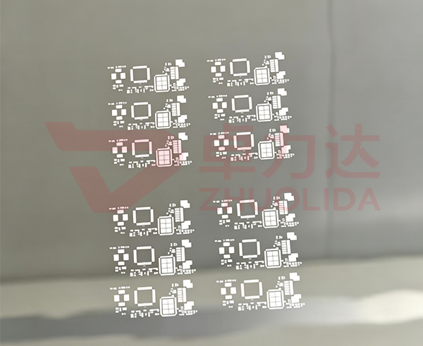
The rapid iteration of FC-BGA and chiplet heterogeneous integration keeps pushing IC substrate I/O density higher, and ultra-fine-pitch pad arrays impose stringent requirements on ball placement, solder paste, and flux printing tooling. Conventional laser and etched stencils rely on subtractive processing, so aperture walls readily develop saw-tooth burrs and side-etch widening; under high-density ball placement conditions they are prone to ball sticking, bridging, insufficient solder, and placement offset, and they may also scratch the fine traces and ABF dielectric layer on the substrate surface, making it hard to meet the mass-production conditions for advanced IC substrates. IC substrate solder ball stencils are formed in a single step by pulsed electroforming of a nickel-cobalt alloy, an additive process with no mechanical cutting stress, high replication accuracy for micro-aperture arrays, and mirror-smooth aperture walls that ensure smooth release of micro solder balls and solder paste, making them indispensable precision tooling for IC substrate packaging. IC substrate solder ball stencil fabrication comprises eight core processes: LDI laser direct imaging platemaking, mother-mold pretreatment, alloy pulsed electroforming deposition, stress-relief annealing, tension calibration and setting, aperture wall mirror polishing, cleanroom washing and passivation, and micron-level full-dimensional inspection. It calls for pattern compensation and parameter tuning tailored to the IC substrate pad layout and the characteristics of the dielectric layer. Grounded in the real pain points of packaging and test lines, IC substrate solder ball stencil manufacturers continuously optimize electroforming chemistries and imaging systems, balancing tooling support for R&D prototypes and volume production.
An IC substrate consists of an organic base material and an ABF dielectric layer, with densely arranged pad arrays and a dielectric surface that resists scratching poorly; even a tiny aperture deviation or residual stress in the IC substrate solder ball stencil can cause interconnect failure across an entire substrate and lead to substantial scrap losses. In standardized IC substrate solder ball stencil fabrication, the pattern transfer stage uses high-precision exposure equipment to fully replicate the micro-aperture array of the substrate pads, applying differentiated pattern compensation to the center and edge regions of the stencil so as to offset the dimensional deviation caused by electroforming undercut and ensure that aperture diameter and aperture position stay highly uniform across the whole panel. The electroforming deposition stage precisely controls pulse current, electrolyte temperature, and circulation flow rate, driving the nickel-cobalt alloy to grow evenly layer by layer and reducing the risk of later deformation caused by uneven grain distribution. The stress-relief process uses temperature-controlled annealing to fully release residual stress inside the stencil, preventing panel warpage and tension drift when heat is applied during printing, and reducing the mechanical friction impact of the squeegee on the IC substrate dielectric layer. IC substrate solder ball stencils can accommodate FC-BGA substrates of multiple specifications and are compatible with different packaging base materials such as ordinary organic substrates and ABF-masked substrates. IC substrate solder ball stencil manufacturers build dedicated process databases for ball-placement arrays of different pitches, reducing the probability of defects such as incomplete apertures and localized over-etching. IC substrate solder ball stencil manufacturers continuously optimize imaging and electroforming parameters to guarantee micro-aperture pattern replication accuracy from the source.
Electroforming deposition and aperture wall treatment are the core steps of IC substrate solder ball stencil fabrication, directly determining how well solder paste and micro solder balls are released as well as the actual service life of the stencil. Stencils produced by conventional subtractive processes have rough aperture walls, so solder paste tends to cling and remain on the walls during printing and high-density micro-apertures clog frequently; production lines must wipe and clean repeatedly, which not only lowers equipment utilization but also raises the risk of scratching substrate traces. IC substrate solder ball stencils are electroformed as a single piece with no joints or seams; aperture tolerance is held at ±1-2 μm and aperture wall roughness at Ra ≤ 0.6 μm, and the inner walls are smooth and vertical, so paste and micro solder balls release smoothly, greatly reducing packaging defects such as ball sticking, solder peaks, solder beading, bridging, and missing prints. The whole forming process is stress-free cold processing with no mechanical squeezing or cutting damage, and the finished panel maintains stable tension at 38-45 N/cm; under long, high-speed printing conditions there is no aperture collapse or panel misalignment. For ultra-fine-pitch ball placement, a nano-coating modification can also be added to lower solder paste adhesion, reduce wiping frequency, and indirectly protect the IC substrate dielectric layer and fine traces. IC substrate solder ball stencil fabrication can form ultra-high-density micro-aperture arrays that are difficult to achieve with conventional processes, breaking through the tooling bottleneck for high-density ball placement on IC substrates. IC substrate solder ball stencil manufacturers have upgraded chemical filtration and circulation systems to reduce micro-aperture defects caused by particulate contamination. IC substrate solder ball stencil manufacturers iterate dynamic process compensation algorithms to further improve dimensional consistency across the whole panel array.
Cleanroom post-processing and full-item inspection are the key closing loop that completes IC substrate solder ball stencil fabrication and safeguards stable pilot and volume production of IC substrate packaging. Electroformed semi-finished products are demolded and peeled in a high-cleanliness environment, and multi-stage ultrapure water circulation washing thoroughly removes electrolyte residue and fine metal debris, preventing hard particles from falling off and scratching IC substrate pads and traces. Surface protection treatment is carried out in line with the actual conditions of packaging and test lines to improve the stencil's wear and corrosion resistance and to support long, uninterrupted printing and ball placement. In the finished-product inspection stage, metallurgical microscopes and 2D vision measuring systems are used for zone-by-zone verification of the whole panel, focusing on aperture diameter, aperture position, tension, and flatness, and screening for microscopic defects such as missing micro-apertures, pattern offset, and localized deformation. All production steps are completed in a semiconductor cleanroom to avoid secondary dust contamination and ensure consistent performance across stencil batches. IC substrate solder ball stencil fabrication strictly follows semiconductor cleanliness control standards and meets the demanding manufacturing conditions for advanced IC substrates. IC substrate solder ball stencil manufacturers strictly implement full inspection and batch-level quality traceability to tightly control outgoing quality. IC substrate solder ball stencil manufacturers continuously optimize cleanroom post-processing flows to raise stencil cleanliness grade and durability.
With the combined advantages of micron-level aperture accuracy, mirror-finish aperture walls, and low residual stress, IC substrate solder ball stencils are widely used in FC-BGA packaging processes for AI computing chips, HBM companion substrates, and high-speed RF chips. In computing-chip applications they suit high-density I/O substrate ball placement printing and ensure interconnect consistency across massive numbers of micro pads; in high-speed RF chips they suit multi-channel fine-pitch array ball placement and ensure the reliability of high-frequency signal interconnects. IC substrate solder ball stencil fabrication covers both R&D prototyping and high-volume production, and stencils can be customized according to the substrate layout and ball placement printing equipment parameters to match the pace of IC substrate packaging technology iteration. Facing the process uncertainty introduced by ultra-fine-pitch arrays, IC substrate solder ball stencil manufacturers rely on DFM manufacturability analysis to identify design-level process risks in advance and shorten the joint validation cycle between stencil and IC substrate. IC substrate solder ball stencil manufacturers keep pace with advanced packaging iteration and keep expanding the application scenarios that stencils can serve.
In summary, as advanced packaging evolves toward ever higher I/O density, conventional stencils can no longer handle the complex conditions of ultra-fine-pitch ball placement on IC substrates; leveraging the unique advantages of additive electroforming, IC substrate solder ball stencils have become important precision tooling on IC substrate packaging and test lines. A mature and complete IC substrate solder ball stencil fabrication system can deliver ball placement stencils with high precision, high cleanliness, and high wear resistance, helping to improve IC substrate packaging yield. IC substrate solder ball stencil manufacturers rely on cleanroom precision production lines to reliably output high-performance packaging stencil products. IC substrate solder ball stencil manufacturers are deeply engaged in the field of semiconductor Precision Electroforming, continuously refining the entire workflow of pattern transfer, electroforming, and cleanliness inspection, providing solid process assurance for the development of the domestic IC substrate packaging industry.
Contact:赖先生
Phone:+86 18938693450
Tel:0755-2708-8292
Email:yw9@zldsmt.com
Add:深圳市宝安区福永镇新和村福园一路华发工业园A3栋
 Zhuolida