Welcome: Shenzhen Zhuolida Electronics Co.TD
Language:
 ∷
∷

∷
∷
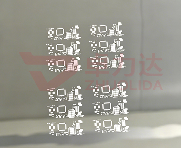
Both electroforming and electroplating belong to electrochemical metal deposition technologies. They share identical underlying electrolytic reaction principles, yet differ completely in process objectives, requirements for core mold / base material, coating thickness, bonding force control and post processing methods. They undertake distinct tasks within semiconductor precision manufacturing. Electroforming and electroplating processes realize metal deposition via reduction and precipitation of metal ions under applied electric fields. Electroplating is a surface modification process, while electroforming represents a metal component forming manufacturing technology. Electroforming and electroplating processes processing shows clear distinctions in electrolyte formulations, power supply modes, stress control and cleanliness standards. Corresponding process routes shall be selected in the semiconductor industry according to product positioning. Electroforming and electroplating processes manufacturers need to fully understand boundary conditions of the two processes and avoid mass volume defects caused by process mismatching, so as to support R&D and mass volume production of MEMS, advanced packaging and substrate manufacturing.
Electroforming and electroplating share basic electrolytic deposition principles. Anode metal and cathode substrate are jointly placed in metal salt electrolyte. After power on, anode metal dissolves into cations, which migrate to cathode surfaces, gain electrons and reduce, gradually generating metal layers on cathode surfaces. In standardized electroforming and electroplating processes processing, finished workpieces serve directly as cathode substrates for electroplating. Thin metal layers firmly adhere to surfaces of original workpieces. Substrates remain permanently after processing, and deposited layers only function as surface coatings of workpieces. For electroforming, strippable master molds act as cathodes. Metals are continuously deposited in thick layers. After forming, metal components must be fully stripped and separated from master molds. Master molds are discarded after replication and are not incorporated into finished products, yielding self supporting independent metal parts.
For electroforming and electroplating processes, electroplating focuses on coating appearance, corrosion resistance and bonding strength with substrates. Electroforming emphasizes replication accuracy on surfaces contacting master molds, together with strict control over overall internal residual stress to facilitate subsequent complete demolding. Electroforming and electroplating processes manufacturers develop differentiated electrolyte formulations for the two processes. Electroplating prioritizes improving coating adhesion; electroforming focuses on lowering internal stress brought by thick layer deposition. Electroforming and electroplating processes manufacturers optimize pulse power supply parameters respectively for semiconductor scenarios to satisfy different requirements of thin coating protection and thick component forming.
Coating thickness and internal stress control constitute core distinguishing points of electroforming and electroplating processes processing and directly determine service performance of products. Electroplating coatings generally range from 1 μm to 50 μm. Thin coatings permit relatively higher residual stress. Their main functions are surface protection, conductive modification and decorative finishing of original workpieces without changing intrinsic structural dimensions of substrates. Electroformed component thickness normally varies from 50 μm to several millimeters. Semiconductor electroformed stencils and wafer templates mostly fall within 80 200 μm. Continuous thick layer deposition readily accumulates residual stress, which will induce warpage or cracking once exceeding thresholds. Therefore, electroforming must adopt pulse power supplies, low stress electrolytes and stress relief annealing procedures to realize low stress monolithic forming without splicing gaps and replicate micron scale micro morphologies of master molds.
For electroforming and electroplating processes, electroplating workpieces require no demolding; coatings bond tightly with substrates. Electroforming demands non destructive overall stripping of formed parts without strong adhesion to master molds. Master mold surfaces need dissociation activation treatment. Electroforming and electroplating processes manufacturers upgrade solution filtration circulation systems. For electroplating, they reduce surface pinhole defects; for electroforming, they reduce internal particle induced defects in thick layers. Electroforming and electroplating processes manufacturers iterate dynamic parameter algorithms. Electroplating pursues uniform coating coverage; electroforming pursues dimensional consistency of full panel arrays.
Post processing and inspection systems form a critical closed loop for electroforming and electroplating processes processing and guarantee yields of semiconductor products. After electroplating, cleaning and passivation are mainly carried out. Inspections focus on coating thickness, adhesion and salt spray corrosion resistance performance, while substrate bodies keep in service. After electroforming, demolding and stripping are completed in high cleanliness workshops, followed by multi stage ultrapure water cleaning, polishing modification and nano coating treatment. Afterwards, micron level inspections are implemented for aperture dimension, aperture position, flatness and tension across full panels to screen defects such as deformation and incomplete micro apertures. Master molds are excluded from finished product links. All semiconductor grade production workflows shall be completed under clean room conditions to avoid particle contamination.
Electroforming and electroplating processes processing strictly complies with semiconductor cleanliness control standards to adapt to different manufacturing procedure conditions. Electroforming and electroplating processes manufacturers enforce full inspection and batch traceability mechanisms to control qualities of electroplated coatings and electroformed component bodies respectively. Electroforming and electroplating processes manufacturers continuously optimize dust free post processing workflows to improve corrosion resistance of electroplated parts and cleanliness durability of electroformed templates respectively.
Due to essential process differences, electroforming and electroplating processes serve completely separated application scenarios within the semiconductor industrial chain. Electroplating is mostly adopted for TSV copper filling of wafers, RDL redistribution, PCB copper foil and gold/nickel plating for device pins. It grows conductive and protective thin layers on original silicon wafers and substrates, acting as surface treatment procedures for chip manufacturing and substrate fabrication. Electroforming is mostly used for semiconductor packaging electroformed stencils, wafer templates, MEMS micro components and micro fluidic devices. It directly manufactures independent precision tooling parts and reproduces high density micro aperture arrays via master molds for OSAT procedures such as ball placement and flux printing.
Electroforming and electroplating processes processing supports both R&D sampling and mass volume production. Electroplating fits surface modification of mass volume substrates; electroforming fits prototyping and customization of complex micro structures and non standard tooling. Confronted with demands for complex micro structures, electroforming and electroplating processes manufacturers apply DFM analysis to identify foreseeable process adaptation risks in advance and avoid material losses caused by improper process selection. Electroforming and electroplating processes manufacturers keep pace with iterations in semiconductor micro nano manufacturing and continuously expand respective adaptation boundaries of the two processes.
In conclusion, electroforming and electroplating processes share homologous electrochemical deposition principles yet feature completely different manufacturing objectives: electroplating “modifies existing workpieces”, while electroforming “grows brand new parts”. Clear boundaries exist in process parameters, thickness requirements, bonding force requirements and application scenarios. Mature electroforming and electroplating processes processing systems can output high performance surface coatings and high precision independent metal components respectively, serving different links of semiconductor manufacturing. Electroforming and electroplating processes manufacturers deliver electroplating modified workpieces and electroformed precision tooling products from dust free precision production lines. Electroforming and electroplating processes manufacturers delve into electrochemical deposition fields, refine complete workflows covering substrate/master mold pretreatment, electrodeposition, post processing and inspection, and deliver solid process guarantees for different manufacturing links of domestic semiconductor industries.
Contact:赖先生
Phone:+86 18938693450
Tel:0755-2708-8292
Email:yw9@zldsmt.com
Add:深圳市宝安区福永镇新和村福园一路华发工业园A3栋
 Zhuolida