Welcome: Shenzhen Zhuolida Electronics Co.TD
Language:
 ∷
∷

∷
∷
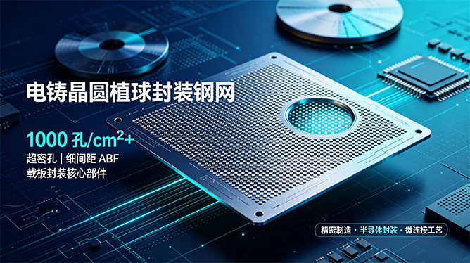
The semiconductor industry is rapidly evolving toward wafer‑level packaging and 2.5D/3D heterogeneous integration, bringing continuous growth in chip I/O pin density. Fine‑pitch ball‑mount processes impose stringent requirements on stencil opening accuracy, aperture wall smoothness and positional tolerance. Conventional laser‑cut and etched stencils suffer from aperture‑wall burrs, opening deformation and excessive dimensional tolerances, which cannot meet mass‑production requirements for high‑end wafer ball mounting. The electroformed wafer ball‑mount stencil is fabricated via layer‑by‑layer electrochemical deposition. Featuring smooth aperture walls, high opening accuracy, low internal stress and excellent wear resistance, it has become an indispensable precision printing tool for advanced packaging production lines. Electroformed wafer ball‑mount stencil processing differs from material‑removal machining methods. Combining photolithographic pattern transfer with electroforming deposition technology, it enables integrated forming of million‑level high‑density micropore arrays and effectively reduces packaging defects such as solder paste residue, solder ball offset and bridging. Electroformed wafer ball‑mount stencil processing manufacturers specializing in semiconductor precision tooling rely on complete process control systems to continuously optimize photolithography, electrolyte and electroforming parameters, delivering stable and reliable stencil solutions for various high‑end chip packaging applications.
Electroformed wafer ball‑mount stencil processing is a dedicated precision manufacturing process for advanced semiconductor packaging and testing. Compared with traditional stencil fabrication, it introduces no mechanical cutting or high‑temperature thermal damage. Finished stencils deliver good flatness and high micropore consistency, suitable for 6‑12‑inch full‑wafer ball‑mount printing. The complete workflow of electroformed wafer ball‑mount stencil processing forms a closed‑loop logic, covering seven core procedures: photolithographic master mold preparation, master mold purification and activation, electroforming electrolyte preparation, electrochemical deposition forming, dynamic process‑parameter control, non‑destructive demolding and precision post‑treatment, and full‑range finished‑product inspection. Every procedure directly affects the opening accuracy, aperture‑wall quality and service life of the electroformed wafer ball‑mount stencil, and serves as a critical control node for electroformed wafer ball‑mount stencil processing manufacturers to guarantee batch yield.
Photolithographic master mold preparation and purification pretreatment constitute the basic procedure of electroformed wafer ball‑mount stencil processing. According to wafer‑packaging drawings including pad arrays, aperture sizes, pitch distances and stencil thickness requirements, photolithography data is processed. Photoresist is evenly coated on conductive substrates, and micropore‑array patterns are transferred through exposure and development to distinguish conductive deposition zones from insulating barrier zones. After master‑mold fabrication, degreasing, repeated pure‑water rinsing and defect repair are performed to remove dust and organic contaminants on the substrate surface, preventing pinholes and partial material shortage during subsequent electroforming. Integrity checks are carried out on insulating patterns to ensure clear boundaries of micropore areas. Professional and standardized electroformed wafer ball‑mount stencil processing manufacturers conduct pattern‑dimension verification for photolithographic master molds and correct minor pattern distortions to control micropore positional and dimensional deviations from the source.
Master‑mold conductive activation and refined electrolyte preparation are vital links to guarantee finished‑product performance for electroformed wafer ball‑mount stencil processing. Photolithographically finished master molds are immersed in special activation solution to activate active sites on conductive zones and improve nickel‑ion adhesion, so as to avoid defects such as insufficient bonding strength of deposited layers and local thinning of coatings. High‑purity nickel‑cobalt alloy electroforming electrolyte is formulated in accordance with stencil hardness, toughness and wear‑resistance requirements. Strict control is implemented over metal‑ion concentration, temperature and pH value. Particulate impurities inside the solution are continuously filtered in circulation, and stress‑regulating additives are added to reduce residual internal stress inside formed stencils. During continuous mass production, electrolyte components are consumed and changed. Electroformed wafer ball‑mount stencil processing manufacturers perform regular sampling and chemical analysis of indicators, dynamically adjust reagent ratios to maintain a stable electrodeposition environment and prevent inter‑batch performance discrepancies.
Electrochemical deposition forming is the core procedure of electroformed wafer ball‑mount stencil processing. Qualified photolithographic master molds are placed as cathodes inside sealed electroforming tanks, with high‑purity nickel‑cobalt alloy adopted as anodes. Key process parameters including current density, stirring rate and deposition duration are precisely set. Driven by a controllable electric field, metal ions are deposited layer‑by‑layer only on exposed conductive zones of master molds to gradually build stencil substrates with complete micropore arrays. This technology supports micron‑level micropore forming with vertical and smooth aperture walls, free of burrs and microcracks induced by mechanical machining. It greatly improves solder‑paste release and reduces printing‑related ball‑mount defects. Experienced electroformed wafer ball‑mount stencil processing manufacturers customize exclusive deposition parameters for different packaging pitches and stencil thicknesses, so as to balance stencil thickness accuracy, structural strength and wear‑resistant service life.
Non‑destructive demolding and precision post‑treatment are key steps to improve the comprehensive performance of electroformed wafer ball‑mount stencils. Once electroformed layers reach preset thickness, non‑destructive demolding methods compatible with master‑mold materials are adopted to gently separate stencils from photolithographic master molds and prevent stencil warpage and micropore deformation caused by pulling. Demolded semi‑finished products go through circulating pure‑water cleaning for electrolyte‑residue removal, low‑temperature stress relief, edge trimming and surface polishing. Some products additionally undergo frame‑mounting and tensioning. The whole post‑treatment workflow must avoid external extrusion to protect high‑density micropore arrays from damage. Standardized electroformed wafer ball‑mount stencil processing manufacturers formulate differentiated post‑treatment schemes for large‑size wafer stencils to control overall stencil flatness and satisfy high‑speed printing alignment requirements.
Comprehensive precision inspection of finished products acts as the final quality‑control checkpoint for electroformed wafer ball‑mount stencil processing. Multi‑dimensional inspections are implemented for electroformed wafer ball‑mount stencils by means of optical microscopic inspection, 3‑D dimensional scanning, aperture‑coordinate verification, aperture‑wall roughness testing, tension and flatness testing. Non‑conforming products with out‑of‑spec apertures, position offsets or surface warpage are rejected, ensuring finished products fully meet stringent accuracy standards for wafer‑level ball‑mount printing.
Benefiting from combined advantages of high precision, low residue and superior wear resistance, electroformed wafer ball‑mount stencils are widely deployed in multiple advanced semiconductor‑packaging scenarios. For logic chips, they are applied to wafer ball‑mount processes of WLCSP and FC‑BGA flip‑chip devices for packaging of AI computing chips and 5G communication chips. For memory chips, they are used in micro‑ball‑mount printing for HBM high‑bandwidth memory and stacked‑memory chips. For automotive semiconductors, they fulfill high‑reliability ball‑mount packaging requirements for automotive‑grade power chips. For MEMS and sensors, they support solder‑paste printing for wafer‑level packaging of micro‑devices.
In summary, electroformed wafer ball‑mount stencil processing effectively addresses multiple technical bottlenecks of conventional stencils for fine‑pitch advanced packaging and serves as a critical precision‑tooling process for the semiconductor packaging‑and‑testing industry. As domestic advanced‑packaging technologies keep upgrading, market demand for high‑density, large‑size electroformed wafer ball‑mount stencils continues to rise. In the future, electroformed wafer ball‑mount stencil processing manufacturers focused on semiconductor precision manufacturing will keep iterating photolithographic patterns, electrolyte systems and electroforming control strategies, further enhancing micropore forming accuracy and production efficiency, and providing solid tooling support for advanced‑packaging development of logic, memory, automotive‑grade, MEMS and other chips.
Contact:赖先生
Phone:+86 18938693450
Tel:0755-2708-8292
Email:yw9@zldsmt.com
Add:深圳市宝安区福永镇新和村福园一路华发工业园A3栋
 Zhuolida