Welcome: Shenzhen Zhuolida Electronics Co.TD
Language:
 ∷
∷

∷
∷
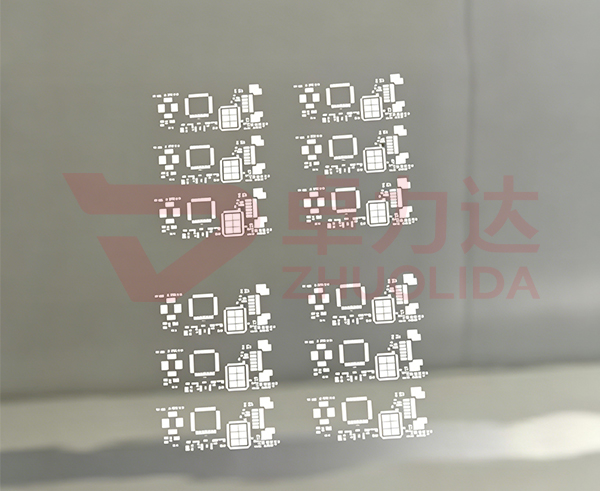
Semiconductor precision manufacturing keeps moving toward miniaturization and high density. Feature sizes of chip circuits and micro bump arrays keep shrinking. Masks fabricated by conventional processes suffer from stress induced deformation, edge burrs and poor dimensional consistency and fail to meet micrometer scale pattern transfer requirements. The semiconductor electroformed mask adopts additive pulse electroforming without mechanical contact, delivers high fidelity pattern reproduction and controllable aperture wall morphology, and serves as vital tooling for chip micro nano processing. Semiconductor electroformed mask processing covers graphic plate making, master mold preparation, alloy electroforming deposition, stress relief annealing, surface polishing, dust free cleaning and micron level comprehensive inspection. Minor fluctuations in each process parameter will directly affect finished product yields of masks. Semiconductor electroformed mask processing manufacturers focus on micrometer scale process challenges, continuously optimize alloy formulas and process systems, and provide reliable supporting services for R&D and mass volume production of precision semiconductor devices.
Micrometer scale patterns impose extremely strict requirements on aperture concentricity, plate surface flatness and tension stability of masks. Tiny dimensional deviations may lead to pattern offset and interconnection failures of subsequent chips and trigger batch scrap of products. Standardized semiconductor electroformed mask processing first prepares master mold patterns via high precision LDI laser direct imaging. Pattern compensation is implemented for micrometer scale micro aperture arrays to offset dimensional deviations caused by electroforming side etching and guarantee highly consistent aperture dimensions and positions for massive micro holes. During electroforming deposition, pulse current density, electrolyte temperature and solution circulation flow rate are precisely controlled for uniform layer by layer deposition of nickel cobalt alloy and eliminate hidden risks of residual internal stress from uneven grain distribution. Stress relief annealing releases internal stress and prevents thermal induced warpage during mask operation, ensuring alignment accuracy for repeated usage. The semiconductor electroformed mask supports diverse micrometer scale pattern requirements and is compatible with application scenarios including advanced packaging, MEMS devices and microfluidic components. Semiconductor electroformed mask processing manufacturers build dedicated process databases for high density micrometer arrays to reduce defect rates of incomplete micro apertures and local over etching. Semiconductor electroformed mask processing manufacturers continuously optimize imaging and electroforming deposition parameters to improve pattern restoration accuracy for micrometer scale features from the source.
Electroforming deposition and aperture wall treatment are core segments of semiconductor electroformed mask processing, directly determining pattern transfer performance and service life of masks. Masks made by conventional subtractive processes have rough inner micro aperture walls, which easily cause material adhesion and aperture clogging during paste printing and pattern transfer, forcing frequent production line shutdowns for cleaning and severely lowering equipment utilization. The semiconductor electroformed mask adopts monolithic electroforming without splicing gaps. Its aperture tolerance reaches ±1~2 μm and aperture wall roughness Ra≤0.6 μm. Smooth vertical inner walls enable easy material release and greatly reduce process defects such as solder dragging, missing printing and pattern distortion. It is a stress free cold forming process free from mechanical extrusion or cutting damage. Finished masks maintain reasonable plate surface tension and avoid aperture collapse and pattern offset after multiple operation cycles. Surface modification can be applied for ultra fine apertures prone to clogging to reduce material adhesion and extend continuous operation cycles. Semiconductor electroformed mask processing realizes high density micrometer array forming unachievable by conventional techniques and removes tooling bottlenecks for semiconductor micrometer scale processing. Semiconductor electroformed mask processing manufacturers upgrade electrolyte filtration circulation systems to reduce micro aperture defects induced by particle impurities. Semiconductor electroformed mask processing manufacturers iterate dynamic process compensation algorithms to further improve overall dimensional consistency of micrometer arrays.
Dust free post processing and comprehensive inspection form a critical closed loop for semiconductor electroformed mask processing and stable mass production of semiconductor precision manufacturing. Electroformed semi finished products are demolded in high cleanliness environments. Multi stage circulating ultrapure water cleaning thoroughly removes residual electrolyte and fine metal debris to prevent device failures caused by falling particles. Surface protection treatments are implemented according to practical working conditions to enhance mask wear resistance and corrosion resistance for long term continuous production. In final inspection, metallographic microscopes and 2D optical measuring instruments verify aperture dimension, position and flatness zone by zone to screen micro defects including damaged micro apertures, pattern offset and local deformation. All workflows are completed in semiconductor grade clean rooms to avoid secondary dust contamination and guarantee consistent batch product performance. Semiconductor electroformed mask processing strictly complies with semiconductor cleanliness specifications for stringent manufacturing conditions for micrometer scale devices. Semiconductor electroformed mask processing manufacturers enforce full inspection and batch quality traceability mechanisms to strictly control outgoing quality. Semiconductor electroformed mask processing manufacturers continuously optimize dust free post processing to further raise mask cleanliness grades and durability.
Benefiting from micrometer level aperture accuracy, smooth aperture walls, low residual stress and excellent array consistency, the semiconductor electroformed mask is widely applied in advanced chip packaging, MEMS sensors, RF devices and microfluidic chips. For advanced packaging, it is deployed for micro bump ball placement and solder paste printing to ensure uniform interconnection of massive micrometer scale micro bumps. For MEMS devices, it supports pattern transfer of micro structures and satisfies miniaturized manufacturing requirements for sensors. Semiconductor electroformed mask processing supports both prototype sampling and mass volume manufacturing. Customization can be completed based on device layouts and equipment parameters to match fast iteration rhythms of the semiconductor industry. For micrometer scale process development, semiconductor electroformed mask processing manufacturers apply DFM analysis to identify foreseeable design induced process risks in advance and cut losses from repeated sampling revisions. Semiconductor electroformed mask processing manufacturers keep pace with advances in semiconductor micro nano manufacturing and continuously expand application boundaries for masks.
In summary, semiconductor manufacturing evolves toward micrometer and sub micrometer scales. Conventional mask processes can no longer satisfy processing requirements for complex micro structures. Leveraging unique electroforming advantages, the semiconductor electroformed mask acts as vital tooling for tackling micrometer scale manufacturing challenges. Mature semiconductor electroformed mask processing systems deliver high precision, high cleanliness and wear resistant electroformed masks and help raise production yields of semiconductor precision devices. Semiconductor electroformed mask processing manufacturers supply high performance masks from dust free precision production lines. Semiconductor electroformed mask processing manufacturers delve into micro nano electroforming technology, refine full workflows covering pattern transfer, electroforming and cleanliness inspection, and deliver solid process support for development of domestic semiconductor precision manufacturing industries.
Contact:赖先生
Phone:+86 18938693450
Tel:0755-2708-8292
Email:yw9@zldsmt.com
Add:深圳市宝安区福永镇新和村福园一路华发工业园A3栋
 Zhuolida