Welcome: Shenzhen Zhuolida Electronics Co.TD
Language:
 ∷
∷

∷
∷
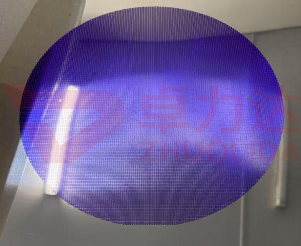
As core precision components for light control, current limiting and optical filtering, slit pieces have strict micron-level requirements for slit straightness, parallelism, wall smoothness and dimensional consistency in high-end fields such as precision optical detection, laser calibration, spectral analysis and industrial vision measurement. Traditional slitting processing methods including laser cutting, chemical etching and stamping often cause burrs, rough wall surfaces, stress deformation and uneven slit width, resulting in light scattering, optical path deviation and detection data errors, which fail to meet the standards of high-precision optical equipment. Precision slit piece electroforming adopts low-stress electrochemical integrated molding technology, eliminating the drawbacks of mechanical cutting and high-temperature processing. It produces ultra-precise slit structures with straight and smooth edges, burr-free surfaces and zero residual stress, becoming the mainstream manufacturing process for high-end slit components. Precision slit piece Electroforming processing is carried out in dust-free and constant-temperature refined production lines. Through pulsed layered deposition, micron-level pattern replication and ultra-clean post-treatment, it effectively solves common industrial problems such as slit edge chipping, width deviation and surface contamination, supporting customized production of ultra-narrow slits, multi-group parallel slits and special-shaped slit pieces. Precision slit piece electroforming processing manufacturers continuously optimize electroforming solution ratio, deposition parameters and surface passivation technology, improving the optical flatness and operational stability of slit pieces and providing reliable technical support for precision optical equipment manufacturing.
Precision slit piece electroforming delivers superior optical molding quality that cannot be achieved by traditional processes, relying on a standardized fully closed-loop precision manufacturing system. The complete workflow covers nine core procedures: high-precision photolithography master mold fabrication, ultra-clean substrate activation, conductive film deposition, pulsed layered electroforming molding, low-temperature stress relief, flexible non-destructive demolding, precision slit polishing and passivation, full-range dimensional inspection, and anti-static dust-free packaging. The parameter accuracy of each procedure directly determines the optical path stability and detection precision of slit pieces. High-precision master mold fabrication serves as the core pre-process of precision slit piece electroforming. According to product specifications of slit width, length, spacing and arrangement, customized low-thermal-expansion and ultra-flat photolithography master molds are adopted. Micro-nano photolithography accurately replicates linear slit structures, and preset micron-level compensation offsets minor lateral erosion loss during electroforming, ensuring consistent slit straightness and dimensional accuracy from the source. Substrate activation thoroughly removes oil stains, dust and oxide impurities on the mold surface to guarantee uniform conductive film adhesion and avoid molding faults such as structural fracture and incomplete slits. Precision slit piece electroforming processing implements intelligent closed-loop control of current density, solution temperature and circulation flow, accurately regulating the ordered growth of nickel grains to ensure smooth and regular slit wall surfaces. Precision slit piece electroforming processing manufacturers build exclusive parameter databases for high-precision scenarios including micron-level ultra-narrow slits and high-density array slits, realizing standardized and stable mass production of various precision slit pieces.
Pulsed layered electroforming molding is the core procedure of precision slit piece electroforming and the key to optical-grade precision slit molding. Adopting low-stress nickel sulfamate solution and high-precision pulse control system, integrated metal molding is completed through layered intermittent deposition. This layered deposition mode continuously releases internal forming stress, thoroughly solving plate warpage and slit deformation caused by residual stress in traditional processing. Finished slits feature vertical and straight edges, smooth and step-free inner walls without burrs, requiring no secondary polishing and fundamentally avoiding precision loss and optical pollution caused by secondary processing. The entire molding process involves no mechanical extrusion or high-temperature thermal damage, leaving no hidden residual stress inside finished products. No slit deviation or plate deformation occurs under long-term light irradiation and alternating temperature conditions, supporting stable long-term continuous operation of precision equipment. Precision slit piece electroforming processing flexibly adapts to the molding of products with different thicknesses and slit specifications, stably achieving micron-level dimensional tolerance and meeting ultra-high-precision application scenarios such as spectral analysis and laser calibration. Precision slit piece electroforming processing manufacturers continuously upgrade the solution circulation and filtration system to reduce slit blockage and surface defects caused by fine metal particle adhesion, effectively improving the optical quality and service life of finished products.
Stress relief, non-destructive demolding and ultra-clean post-treatment are critical closed-loop procedures that ensure the long-term stability of finished products from precision slit piece electroforming. After reaching the preset electroforming thickness, semi-finished products are transferred to low-temperature constant-temperature chambers for prolonged stress elimination treatment. This process further releases residual stress, enhances the flatness and deformation resistance of slit pieces, and prevents precision deviation caused by equipment vibration and ambient temperature changes. The flexible non-destructive demolding process gently separates molded components from master molds, avoiding slit tensile deformation and edge distortion caused by forced stripping and completely retaining the original precision of micro slits. After demolding, multi-stage ultrapure water circulation cleaning, precise slit dredging and anti-oxidation passivation form a dense and uniform protective film on the product surface, improving oxidation resistance and anti-aging performance and preventing surface graying and optical path interference during long-term operation. All finished products undergo full-dimensional quality inspection via high-precision optical measuring instruments, flatness testers and micron-level aperture detectors to eliminate defective products such as curved slits, uneven width and surface flaws. Qualified products are vacuum-packaged in Class 100 dust-free environments. Precision slit piece electroforming processing relies on full-process refined quality control to ensure qualified optical performance and dimensional accuracy. Precision slit piece electroforming processing manufacturers strictly implement piece-by-piece full inspection and batch sampling systems, establish a complete quality traceability system, and ensure unified accuracy and stable performance of batch products.
Featuring high flatness, zero stress, burr-free surface and excellent optical performance, precision slit piece electroforming is widely applied in high-end manufacturing fields including precision optical instruments, laser equipment, spectral detection, industrial vision, medical imaging and precision sensing. In the field of optical detection, electroformed precision slit pieces accurately constrain optical paths and filter stray light, improving the detection accuracy and data stability of spectrometers and spectrophotometers. In laser precision processing, standardized slit structures realize precise laser beam calibration and shaping, ensuring the processing accuracy of laser cutting and laser engraving. In industrial vision, slit pieces precisely control light intake, eliminate ambient stray light interference, and improve the imaging clarity and recognition accuracy of machine vision detection and precision dimension measurement. In medical imaging, high-precision clean slit components adapt to medical imaging equipment, ensuring uniform and clear imaging quality and meeting medical precision detection standards. Precision slit piece electroforming processing can customize various structures such as single slits, multi-group parallel slits and array slits according to different equipment working conditions, flexibly adapting to new product research sampling and large-scale mass production. Precision slit piece electroforming processing manufacturers continuously iterate and optimize process parameters based on working conditions of various precision equipment, improving slit molding accuracy and optical stability to empower the upgrading of high-end precision detection industries.
In conclusion, precision slit piece electroforming thoroughly breaks through the technical bottlenecks of traditional slit processing, including insufficient precision, easy deformation and severe optical interference, becoming an indispensable core manufacturing process for precision components in modern precision optics and precision detection industries. Relying on a standardized dust-free, constant-temperature and low-stress electroforming system, precision slit piece electroforming processing realizes batch mass production and stable delivery of high-precision, high-stability and high-cleanliness precision slit pieces. Precision slit piece electroforming processing manufacturers continue to deepen core electroforming technologies, optimize key processes including slit molding, stress regulation and optical-grade post-treatment, improve the comprehensive service performance of precision slit pieces, and provide solid process guarantees for the high-quality development of high-end precision optics and intelligent detection industries.
Contact:赖先生
Phone:+86 18938693450
Tel:0755-2708-8292
Email:yw9@zldsmt.com
Add:深圳市宝安区福永镇新和村福园一路华发工业园A3栋
 Zhuolida