Welcome: Shenzhen Zhuolida Electronics Co.TD
Language:
 ∷
∷

∷
∷
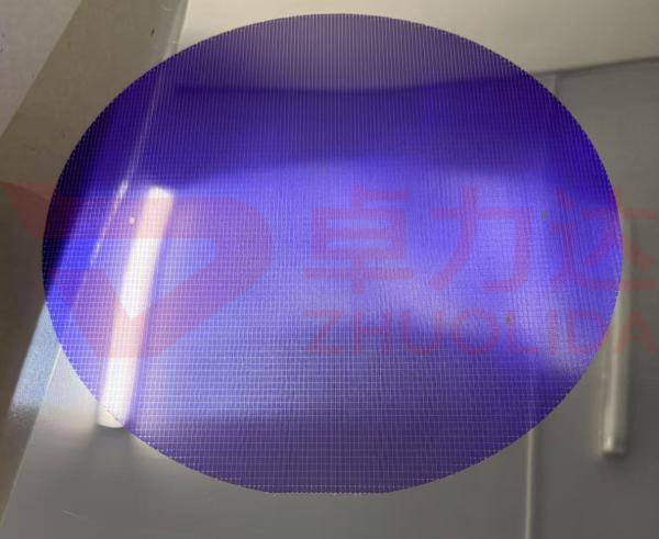
In the field of semiconductor packaging and testing, the precision requirements for metal templates used in wafer-level testing, probe cards, and precision carriers are constantly increasing. Wafer templates developed for 8-inch wafer production lines must maintain excellent dimensional consistency and profile control at pattern sizes of tens of microns. At this point, the 8-inch wafer template electroforming process for semiconductor packaging and testing, with its advantages of high pattern accuracy, smooth sidewalls, and low internal stress, is becoming the mainstream approach for manufacturing precision metal templates in the packaging and testing industry. Compared with mechanical machining, the electroforming process is not limited by material hardness and can achieve batch replication of complex patterns, which is why it is widely applied in packaging and testing applications.
To understand the electroforming process, it is essential to first look at its prerequisite stage — pattern design and core mold preparation. After the customer provides design drawings, process engineers apply dimensional compensation to the patterns, converting factors such as electroforming deposition uniformity and pattern shrinkage into the original files, and then transfer the patterns onto a photoresist layer coated on the substrate using laser direct writing or high-resolution photoplotting equipment. After developing, the substrate surface forms window structures exactly matching the target patterns, and this substrate serves as the core mold for subsequent electroforming deposition. The quality of the core mold output at this stage directly determines the overall precision level of the subsequent 8-inch wafer template processing for semiconductor packaging and testing. Therefore, the cleaning, baking, and contamination control of the core mold must not be taken lightly.
Once the core mold is ready, the photolithographic patterning stage begins. The substrate first undergoes strict chemical cleaning and drying, then a uniform photoresist layer is applied by spin coating, followed by soft baking to remove solvents and stabilize the film. In the exposure step, high-precision alignment equipment projects the designed pattern precisely onto the photoresist layer, and after developing, open windows matching the design are obtained. This step is a key node of precision control in 8-inch wafer template processing for semiconductor packaging and testing. Any dust particles in the cleanroom or minor fluctuations in exposure energy can leave irreversible defects on the final product, which is why this stage is typically carried out in workshops with a higher cleanliness rating.
Next comes the core of the entire process — electroforming deposition. For the 8-inch wafer template electroforming process for semiconductor packaging and testing, the electroforming bath typically uses nickel sulfamate or nickel sulfate electrolyte. Under constant temperature and constant current conditions, nickel ions are reduced and deposited layer by layer within the windows of the core mold until the target thickness is reached. To ensure thickness uniformity, the industry commonly adopts cathode oscillation combined with multi-zone anode layouts, and pulse current is applied to control grain size and internal stress. During deposition, the current density, temperature, pH value, and nickel ion concentration must all be monitored in real time, as any parameter drift can cause thickness deviation or pinhole defects. It can be said that the success of the 8-inch wafer template electroforming process for semiconductor packaging and testing largely depends on the stability of the electroforming parameter window, which is the core of each manufacturer's process know-how.
The stripping stage after deposition is equally demanding. Through chemical swelling or mechanical stripping, the electroformed layer is separated from the core mold to obtain a metal template with precision through-holes or patterns. Subsequently, resist removal, ultrasonic cleaning, and deburring are carried out in sequence to remove edge residues and burrs. For products with high wear resistance requirements, surface hardening or coating treatment may also be applied to extend the service life of the template. The entire post-processing routine must be gentle and controllable to avoid secondary damage to the precision patterns.
Quality inspection runs through the entire 8-inch wafer template processing for semiconductor packaging and testing. Vision measuring machines are used to measure hole position coordinates and line width dimensions, while profilometers and metallurgical microscopes are used to examine cross-sectional morphology and sidewall verticality, and thickness gauges perform multi-point sampling of the overall thickness distribution. Only products whose dimensions, morphology, and surface roughness all meet the requirements can enter the packaging stage and be delivered to customers with dust-free protection.
It is worth noting that 8-inch wafer template processing for semiconductor packaging and testing places strict requirements on the production environment. The photolithography and electroforming processes are usually arranged in cleanrooms rated at Class 1,000 or even Class 100 to reduce the risk of foreign particle contamination at the source. Meanwhile, different customers have different requirements for template hardness, corrosion resistance, and service life, so suppliers need complete process verification and small-batch trial production capabilities to fully expose and resolve potential issues before product delivery.
When selecting an 8-inch wafer template electroforming process for semiconductor packaging and testing, it is recommended to focus on three capabilities: first, measured data on pattern accuracy and thickness uniformity; second, the response speed of sample trial production; and third, yield and delivery stability in mass production. Manufacturers with a complete production chain are often able to achieve a better balance between cost and quality, providing long-term and stable supply assurance for packaging and testing customers.
As advanced packaging evolves toward finer patterns and larger sizes, the demand for the 8-inch wafer template electroforming process for semiconductor packaging and testing is expected to continue growing. Overall, 8-inch wafer template processing for semiconductor packaging and testing is moving toward higher precision and faster delivery, and the maturity of the electroforming process will further lower the entry barrier for advanced packaging products. It is foreseeable that the electroforming process will be deeply integrated with laser processing, precision etching, and other technologies, providing the packaging and testing industry with wafer template solutions of higher precision and longer service life. For buyers, establishing cooperation with suppliers that have electroforming process capabilities as early as possible will help them take the lead in product iteration and cost reduction.
Contact:赖先生
Phone:+86 18938693450
Tel:0755-2708-8292
Email:yw9@zldsmt.com
Add:深圳市宝安区福永镇新和村福园一路华发工业园A3栋
 Zhuolida