Welcome: Shenzhen Zhuolida Electronics Co.TD
Language:
 ∷
∷

∷
∷
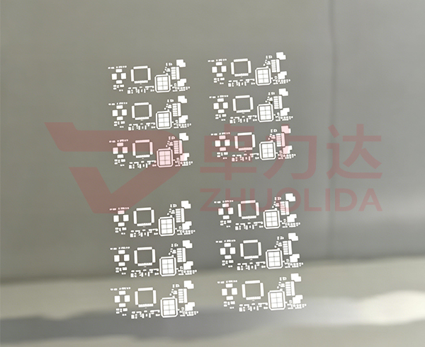
As advanced packaging and wafer-level testing technologies migrate to 12-inch production lines, the demand for large-size wafer templates is growing rapidly. Compared with 8-inch products, 12-inch wafer templates have a larger area and more patterns, imposing stricter requirements on dimensional consistency, warpage, and surface quality. Against this backdrop, the 12-inch wafer template electroforming process for semiconductor packaging and testing, with its advantages of high pattern accuracy, controllable internal stress, and excellent batch replication consistency, has become an important process route for manufacturing large-size precision metal templates. The electroforming process is not limited by material hardness and is especially suitable for producing test carriers and template parts with dense through-holes and fine patterns.
The first step in the electroforming process is pattern design and core mold preparation. After the customer drawings are evaluated by process engineers, zonal compensation is applied to the large-area patterns, converting factors such as electroforming deposition uniformity, pattern shrinkage, and edge effects into the design files. The patterns are then transferred onto a photoresist layer on the substrate using laser direct writing or high-resolution photoplotting equipment. After developing, the window structures formed on the substrate serve as the core mold for subsequent deposition. For 12-inch products, the core mold is large and susceptible to temperature and humidity variations, so environmental conditions must be strictly controlled from cleaning and baking to handling. The quality of the core mold output at this stage directly determines the overall precision level of the subsequent 12-inch wafer template processing for semiconductor packaging and testing.
Once the core mold is complete, the photolithographic patterning stage begins. After chemical cleaning and drying, photoresist is applied to the substrate by spin coating, followed by soft baking to stabilize the film. Because of the larger pattern area, exposure of 12-inch wafer templates usually relies on stepper or scanning exposure equipment, which projects the design pattern onto the resist layer region by region; after developing, open windows matching the design are obtained. This step is a key node of precision control in 12-inch wafer template processing for semiconductor packaging and testing. Edge exposure non-uniformity and cumulative alignment errors caused by the large format must be suppressed through compensation parameters, which is why this stage is typically carried out in Class 100 cleanroom environments.
Next comes the core of the entire process — electroforming deposition. For the 12-inch wafer template electroforming process for semiconductor packaging and testing, the electroforming bath typically uses nickel sulfamate electrolyte, equipped with a larger anode area and a more uniform flow field design to ensure thickness consistency over the large-area substrate. During deposition, the current density, temperature, pH value, and nickel ion concentration must be monitored online, and internal stress and warpage are suppressed through cathode oscillation combined with zoned current control and pulse power supply. For 12-inch products, in-plane thickness uniformity is the biggest process challenge; any parameter drift can cause edge thickening or a thinner center. It can be said that the success of the 12-inch wafer template electroforming process for semiconductor packaging and testing depends on the stability of the electroforming parameter window and the uniformity compensation model.
The stripping stage after deposition is equally critical. Through chemical swelling or mechanical stripping, the electroformed layer is separated from the core mold to obtain a metal template with precision through-holes or patterns. Subsequently, resist removal, ultrasonic cleaning, and deburring are carried out to remove edge residues; for products with high wear resistance requirements, surface hardening or coating treatment may also be applied to extend service life. Large-size templates are more prone to deformation during post-processing and handling, so every step emphasizes a gentle and stable approach.
Quality inspection runs through the entire 12-inch wafer template processing for semiconductor packaging and testing. Vision measuring machines measure hole position coordinates and line width dimensions, while profilometers and metallurgical microscopes examine cross-sectional morphology and sidewall verticality, and laser thickness gauges or multi-point measuring equipment sample the overall thickness distribution; warpage inspection is equally indispensable. Only products whose dimensions, morphology, and surface quality all meet the requirements can enter the packaging stage and be delivered with dust-free protection.
It is worth noting that 12-inch wafer template processing for semiconductor packaging and testing places high demands on the production environment and equipment capability. The photolithography and electroforming processes are usually arranged in Class 100 or Class 1,000 cleanrooms to reduce the risk of foreign particle contamination at the source. In addition, manufacturing large-size templates requires large-area exposure equipment, high-capacity electroforming baths, and automated handling systems, so both hardware investment and process know-how are indispensable for suppliers.
When selecting a 12-inch wafer template electroforming process for semiconductor packaging and testing, it is recommended to focus on three capabilities: first, measured data on large-area thickness uniformity and warpage control; second, the response speed of sample trial production; and third, yield and delivery stability in mass production. Only manufacturers with a complete production line and sufficient process verification experience can provide reliable supply assurance for packaging and testing customers.
As 12-inch production lines become more prevalent in advanced packaging and wafer-level testing, the demand for the 12-inch wafer template electroforming process for semiconductor packaging and testing will continue to grow. Overall, 12-inch wafer template processing for semiconductor packaging and testing is moving toward thinner, flatter, and more precise products, and the integration of electroforming with laser processing and precision etching will further expand the application boundaries of large-size templates. For buyers, locking in suppliers with large-size electroforming capabilities as early as possible will help them gain an advantage in product upgrades and cost reduction.
Contact:赖先生
Phone:+86 18938693450
Tel:0755-2708-8292
Email:yw9@zldsmt.com
Add:深圳市宝安区福永镇新和村福园一路华发工业园A3栋
 Zhuolida