Welcome: Shenzhen Zhuolida Electronics Co.TD
Language:
 ∷

∷
∷
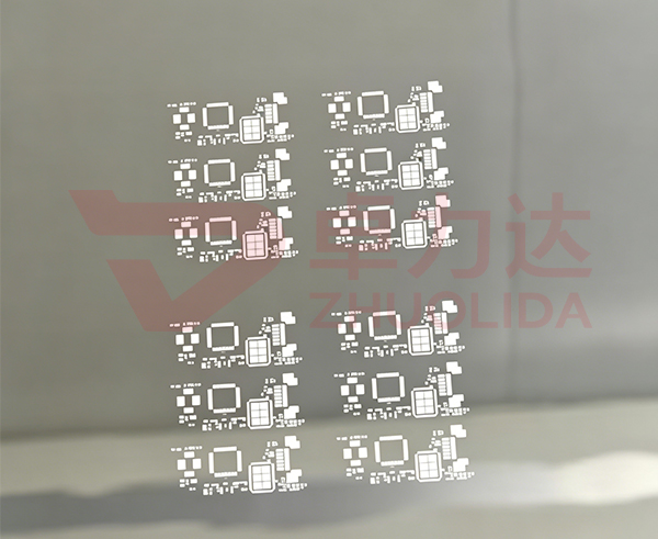
The stencil is the precision tool that transfers solder paste or flux onto pads during semiconductor packaging and SMT assembly. Two forming routes dominate the market: the electroformed stencil and the etched stencil. Both serve printing, yet they differ fundamentally in forming principle, hole-wall morphology, aperture accuracy, residual stress and cost structure. Electroformed stencils are built additively by electrochemical deposition and deliver vertical, mirror-smooth hole walls with virtually no undercut. Etched stencils are formed subtractively by chemical dissolution and offer mature processing at lower cost, though undercut limits their precision for ultra-fine-pitch arrays. Understanding this electroformed vs etched stencil comparison guides correct tool selection across advanced packaging and general electronics assembly.
Dimension | Electroformed Stencil | Etched Stencil |
Forming principle | Additive metal deposition on master mold | Subtractive chemical dissolution |
Hole-wall profile | Vertical, mirror-smooth (Ra ≤ 0.6 µm) | Tapered by undercut, rougher (Ra ≈ 0.8–1.5 µm) |
Aperture tolerance | ±1–2 µm | ±3–5 µm |
Side-etch / taper | None | Inherent, needs compensation |
Residual stress | Low, released by annealing | Redistributed during etch |
Panel tension | Stable 38–45 N/cm | Less controlled |
Wear & life | Nickel-cobalt alloy, hard, coatable | Shorter, hole erosion over time |
Unit cost | Higher | Lower |
Best fit | Fine pitch, high density, advanced packaging | General SMT, prototyping, larger features |
Electroformed stencils grow the metal layer-by-layer on a patterned conductive master mold. Because no chemical undercut occurs, hole walls are vertical and smooth, so solder paste releases cleanly without adhesion or clogging. Aperture tolerance of ±1–2 µm and stable panel tension support ultra-fine-pitch ball placement and solder-paste transfer with minimal bridging, insufficient-solder or solder-drag defects. Low residual stress prevents warpage and tension drift under repeated high-speed printing, protecting brittle substrates.
Etched stencils use photochemical etching: a photosensitive mask is patterned and the exposed metal is dissolved by etchant. The process is mature, fast and affordable, with no expensive tooling changes. It suits larger apertures, moderate precision and high-volume production where unit cost matters. Flexible pattern changes require only artwork revisions, making etched stencils ideal for prototyping and quick turnaround on general SMT lines.
Fine pitch below 0.3 mm where taper causes yield loss
High-density ball placement for FC-BGA, CoWoS and glass substrates
Long-duration high-speed printing needing stable tension and low wear
Products demanding vertical hole walls and minimal solder drag
General SMT solder-paste printing with moderate precision
Prototype development and fast design iterations
Cost-sensitive, high-volume runs with larger apertures
Applications where undercut compensation is acceptable
Vertical hole walls: No undercut, cleaner paste release and less clogging.
Higher aperture accuracy: ±1–2 µm supports ultra-fine-pitch arrays.
Lower residual stress: Annealed for stable tension and no warpage.
Longer service life: Harder nickel-cobalt alloy, optional nano-coating.
Fewer defects: Reduced bridging, insufficient solder and solder beads.
Higher yields at fine pitch: Precision that etched stencils cannot match.
Electroformed: FC-BGA ball masks, CoWoS 2.5D stencils, glass-substrate templates, u-ball flux printing
Etched: SMT solder-paste stencils, general PCB assembly, lead-frame and simple mask parts
Select electroformed for pitch below 0.3 mm or high I/O density.
Apply undercut compensation on etched designs before artwork release.
Match stencil thickness to solder-paste volume and pad size.
Verify panel tension and flatness for large-area printing.
Consider nano-coating to reduce wiping frequency in fine-pitch runs.
Contact:赖先生
Phone:+86 18938693450
Tel:0755-2708-8292
Email:yw9@zldsmt.com
Add:深圳市宝安区福永镇新和村福园一路华发工业园A3栋
 Zhuolida