Welcome: Shenzhen Zhuolida Electronics Co.TD
Language:
 ∷

∷
∷
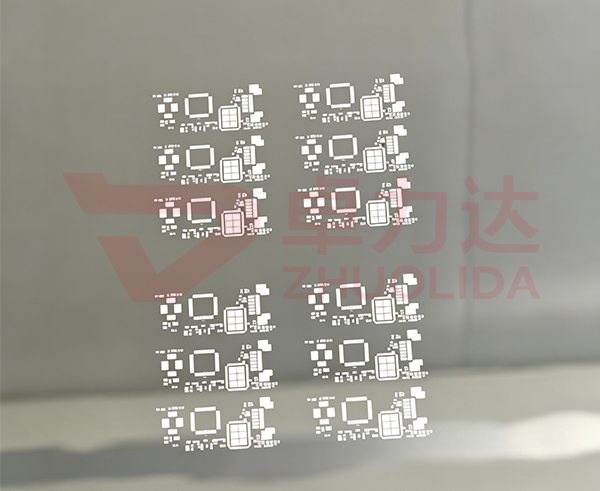
The wafer metal etched template is a precision metal mask used across wafer-level packaging and advanced packaging-and-testing processes. It is formed by photochemical etching: a thin metal foil is coated with photosensitive film, patterned by exposure and development, then dissolved selectively by etchant to create micron-level openings, shaped windows and dense arrays. Because chemical etching applies no mechanical force and no processing stress, thin templates resist deformation and support repeated use on wafer-level lines. The template governs solder-paste volume, flux distribution, plating coverage and coating accuracy, directly driving micro-joint consistency and packaging yield. Its aperture dimension, hole position, flatness and edge quality are the key control points for every wafer-level application.
Available Materials: stainless steel, nickel-based alloy, copper alloy
Material Thickness Range: 0.03–0.3 mm
Aperture Tolerance: ±3–5 µm
Minimum Feature: 1.2–1.5 × material thickness
Surface / Edge Quality: burr-free, smooth edges
Compliance: semiconductor-grade cleanliness
Material Selection & Pre-treatment — Choose low-stress foil; degrease, pickle and activate the surface.
Dry Film Lamination — Laminate photosensitive film on both faces under controlled temperature and pressure.
UV Exposure / LDI — Transfer wafer pad arrays and openings to the photosensitive layer.
Development — Wash away unexposed film to expose regions for etching.
Controlled Chemical Etching (Core Step) — Double-sided spray etching; tune concentration, temperature and pressure to stabilize undercut.
Resist Stripping & Cleaning — Remove the mask, multi-stage rinse and dry.
Post-treatment — Passivation, polishing and precision cleaning per wafer-level cleanliness.
Full Inspection — Verify aperture, position, flatness and edge burrs hole-by-hole.
Stress-free forming: No mechanical impact, thin templates stay flat.
Micron-level patterns: Small apertures, shaped windows and dense arrays.
Design flexibility: Pattern changes only require artwork revisions.
Cost-effective: Mature process, low unit cost, short lead time.
Wide material range: Stainless, nickel-based and copper alloys.
Clean, burr-free edges: Reduces contamination in clean wafer processes.
Wafer ball placement and solder-paste printing
WLP solder-paste stencils
RDL (redistribution layer) masks
UBM electroplating masks
Coating and developing masks
Selective plating and etching masks
Apply hole-position compensation to offset undercut and printing deformation.
Keep minimum feature at 1.2–1.5 × foil thickness for reliable etching.
Match template thickness to solder-paste volume and pad geometry.
Optimize hole-wall verticality for ultra-fine-pitch ball placement.
Verify flatness to ensure uniform printing pressure across the wafer.
Enforce semiconductor-grade cleanliness to avoid particle defects.
Contact:赖先生
Phone:+86 18938693450
Tel:0755-2708-8292
Email:yw9@zldsmt.com
Add:深圳市宝安区福永镇新和村福园一路华发工业园A3栋
 Zhuolida