Welcome: Shenzhen Zhuolida Electronics Co.TD
Language:
 ∷

∷
∷
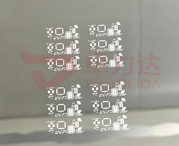
An electroformed photovoltaic mesh is a precision nickel or nickel-cobalt micro-metal template used to deposit, pattern, or screen-print the fine grid fingers that collect current on the front side of crystalline silicon solar cells and heterojunction modules. Unlike etched or laser-cut grids, it is built by additive electroforming—growing a thin, stress-free metal shell around a patterned mandrel—so the resulting apertures are nearly vertical, smooth, and reproducible at micron scale. This makes it a critical tool as cells move toward higher efficiency, narrower busbars, and lower silver consumption. The process supports stainless steel, pure nickel, and nickel-cobalt alloys across thicknesses from 30 µm to 300 µm, with aperture tolerance in the single-digit micrometer range.
Parameter Window
• Available Materials: Pure nickel, nickel-cobalt alloy, stainless steel
• Material Thickness Range: 0.03–0.30 mm
• Aperture Tolerance: ±1–3 µm
• Minimum Feature: ≈ 1.0–1.2 × material thickness
• Surface / Hole-Wall Quality: Hole-wall Ra ≤ 0.6 µm, vertical sidewalls
• Compliance: RoHS / ISO cleanroom compatible
Manufacturing Process / Workflow (8 Steps)
1. DFM & Artwork Review — Translate cell metallization layout into grid-finger compensation drawings, accounting for finger width, pitch, and busbar routing.
2. Surface Pre-treatment — Degrease, acid-clean, and activate the mandrel substrate to ensure uniform deposition.
3. Dry Film Lamination & Exposure — Laminate photoresist and transfer the grid pattern by UV or LDI lithography.
4. Development — Reveal the precision aperture windows that will become the grid openings.
5. Pulse Electroforming Deposition (Core Step) — Grow nickel or nickel-cobalt layer by controlled pulsed current, building vertical, low-stress sidewalls.
6. Stress Relief & Demolding — Anneal to release residual stress, then separate the free-standing mesh from the mandrel.
7. Tension Setting & Edge Processing — Mount onto a frame, tension to specification, and finish the edges.
8. Cleaning & Micro-hole Inspection — Class-100 clean wash followed by microscopy and dimensional inspection.
Core Advantages
1. Near-Vertical, Smooth Sidewalls — Electroformed apertures have minimal taper and low roughness, so paste or material transfers cleanly without bridging.
2. Ultra-Fine Finger Reproducibility — Pitch and width hold at micron scale, enabling narrower fingers that reduce shading and silver use.
3. Low Residual Stress — Pulsed deposition plus annealing yields a flat, dimensionally stable mesh that resists warping under tension.
4. Excellent Wear and Release — Nickel-cobalt alloy is hard and durable; optional nano-coating reduces paste adhesion and extends stencil life.
5. No Mechanical or Thermal Damage — Additive electroforming avoids burrs, heat-affected zones, and micro-cracks associated with stamping or laser cutting.
6. Design Flexibility for High Efficiency — Pattern changes are made in artwork, not hard tooling, supporting rapid iteration for busbar-less and multi-busbar cells.
Typical Applications
• Crystalline Silicon Cells — Front-side silver paste printing and finger definition.
• Heterojunction (HJT) Modules — Low-stress contact for transparent conductive oxide metallization.
• PERC / TOPCon Cells — Fine-line grid printing to cut shading loss.
• Shingled & Busbar-less Designs — Precision aperture arrays for narrow, high-density fingers.
• R&D and Pilot Lines — Fast-turn artwork for new cell architectures.
• Recycled-Silver and Low-Ag Processes — Controlled deposit volume per aperture.
Design Notes & Process Considerations
1. Compensate artwork for finger spread and paste rheology so printed line width matches cell design targets.
2. Balance mesh thickness against aperture area—too thin lowers durability, too thick increases deposit volume.
3. Specify nickel-cobalt alloy for high-cycle production; use pure nickel for prototyping and lower wear.
4. Keep tension uniform across the frame to avoid positional drift of outer apertures.
5. Validate aperture cleanliness and partial blocking before each production run.
6. Pair with matched paste viscosity and print pressure for stable transfer across the full panel.
Contact:赖先生
Phone:+86 18938693450
Tel:0755-2708-8292
Email:yw9@zldsmt.com
Add:深圳市宝安区福永镇新和村福园一路华发工业园A3栋
 Zhuolida