Welcome: Shenzhen Zhuolida Electronics Co.TD
Language:
 ∷
∷

∷
∷
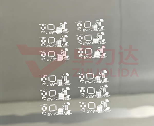
Dongguan Electroformed Wafer Steel Screens, Dongguan Electroformed Wafer Steel Screen Fabrication, Dongguan Electroformed Wafer Steel Screen Manufacturers
Relying on the industrial cluster advantages of semiconductor packaging and testing in the Pearl River Delta, the high-end precision electronic manufacturing industry in Dongguan has been continuously upgraded. Wafer-level packaging, chip ball placement and micro-pitch mounting processes are gradually developing toward ultra-fine aperture, ultra-high uniformity and zero-defect printing. Traditional etched and laser-processed wafer stencils can no longer meet the production requirements of advanced packaging. Conventionally processed stencils commonly suffer from step-shaped hole walls, aperture deviation, residual board stress and deformation after long-term printing, which easily cause defective issues such as uneven wafer solder paste coating, ball placement offset and packaging voids. Dongguan electroformed wafer stencils adopt low-stress electrochemical additive molding technology. With the advantages of vertical and smooth openings, uniform thickness, high array accuracy and zero mechanical deformation, they have become core supporting tooling for local high-precision semiconductor packaging. Dongguan electroformed wafer stencil processing relies on a local ultra-clean production system, adapts to small and medium batch customization and large-scale mass production, and can accurately match the precision printing process standards of various wafers. Dongguan electroformed wafer stencil processors cater to the needs of the local semiconductor industry, continuously optimize electroforming formulas and micro-nano molding parameters, solve industrial difficulties including difficult molding of high-density micropores and poor printing consistency, and provide process support for the quality upgrading of the packaging and testing industry in and around Dongguan.
As core precision molds for chip packaging, wafer stencils have strict micron-level requirements for micropore alignment accuracy, board flatness and hole wall smoothness, with an extremely low processing error tolerance. The complete workflow of Dongguan electroformed wafer stencil processing is implemented in a closed-loop environment of constant temperature, Class 100 ultra-clean and light-shielded dust-free workshops in strict accordance with semiconductor precision manufacturing specifications. It covers nine core processes: high-precision photolithography master mold preparation, substrate ultra-clean activation, uniform conductive film deposition, pulsed layered nickel electroforming molding, low-temperature stress relief, non-destructive demoulding and separation, micropore passivation and trimming, full-range precision inspection, and anti-static vacuum packaging. Throughout the production process, current density, solution circulation rate and molding temperature are intelligently adjusted to precisely control the growth rhythm of metal grains, effectively avoiding processing defects such as elliptical micropores, board warpage, uneven thickness and rough hole walls. Dongguan electroformed wafer stencils are molded from high-purity nickel materials, featuring dense structure, balanced toughness and excellent fatigue resistance, suitable for long-term high-frequency printing operations in semiconductor production lines. Dongguan electroformed wafer stencil processors establish differentiated process standards based on local mainstream packaging technologies, adapting to the processing demands of various wafers including memory wafers, logic chips and power chips.
High-precision master mold preparation and ultra-clean pretreatment are core pre-processes that guarantee the molding accuracy ofDongguan electroformed wafer stencil processing. The position accuracy, aperture size and arrangement regularity of wafer micropore arrays are completely replicated from master molds. Before production, high-precision negative master molds are manufactured through micro-nano photolithography and precision shaping according to wafer layout parameters and packaging process requirements, thoroughly eliminating hole position deviation, array misalignment and hole shape distortion. Low-deformation and high-stability substrates are adopted for master mold production. Multi-stage degreasing and decontamination, circulating ultrapure water rinsing and plasma activation purification are performed to completely remove surface dust and oxide impurities, ensuring an ultra-clean master mold surface and laying a solid foundation for uniform nickel ion deposition. For high-density ultra-fine micropore structures, micro-size compensation design is adopted in advance to offset tiny lateral erosion deviation during electroforming and ensure vertical and regular openings. Dongguan electroformed wafer stencils achieve stable micron-level packaging printing accuracy through high-precision master mold replication, meeting the stringent standards of advanced packaging.Dongguan electroformed wafer stencil processors refine master mold preparation and maintenance specifications, reduce the defective rate of stencil molding from the source, and ensure consistent accuracy of mass-produced products.
Pulsed electroforming deposition and stress relief treatment are the core molding procedures of Dongguan electroformed wafer stencil processing. The pretreated master mold is coated with a uniform and dense conductive film in an ultra-clean workstation to build a stable conductive substrate, ensuring ordered stacking and growth of nickel ions and avoiding local deposition fracture, incomplete micropores and uneven board thickness. The master mold is placed in a sealed constant-temperature electroforming tank filled with semiconductor-grade low-stress special solution, paired with a high-precision pulse current control system to realize slow and dense molding of metal grains. The layered intermittent deposition mode continuously releases molding stress, delivering stencils with flat surfaces, uniform tension and smooth step-free micropore inner walls without secondary hole polishing. The molded semi-finished products undergo low-temperature constant-temperature stress relief to completely eliminate subtle internal stress, greatly improving the deformation resistance of stencils and preventing accuracy deviation caused by long-term printing vibration and temperature fluctuation. Dongguan electroformed wafer stencils feature no mechanical processing damage or residual stress, with clean solder paste demoulding and uniform coating, adapting to high-precision wafer-level packaging processes. Dongguan electroformed wafer stencil processors continuously iterate pulse deposition technology, effectively solving industrial pain points such as uneven molding of dense micropores, solder paste adhesion and hole blockage.
Non-destructive demoulding, surface modification and precision inspection are key procedures to improve the finished performance and stability of Dongguan electroformed wafer stencil processing. After molding, a mild non-destructive demoulding process is adopted to stably separate stencils from master molds, avoiding micropore stretching, board wrinkles and structural deformation caused by forced demoulding. Post-demoulding ultra-clean fine cleaning, micropore dredging and anti-oxidation passivation optimize hole wall smoothness, reduce solder paste residue and micropore blockage, and significantly improve the service life and printing consistency of stencils. High-precision image detectors, aperture uniformity testers and flatness testing equipment are used for full-dimensional verification of stencil dimensional accuracy, micropore verticality and hole pitch consistency to strictly screen out defective products. Qualified finished products are packaged with anti-static and moisture-proof vacuum in dust-free workstations to prevent dust pollution and oxidation failure during storage and transportation. With multi-layer quality control, Dongguan electroformed wafer stencils fully adapt to the dust-free mass production working conditions of high-end semiconductors. Dongguan electroformed wafer stencil processors build a full-process quality control system to realize controllable product parameters and stable quality, fitting the large-scale production needs of the local packaging and testing industry.
In terms of industrial application,Dongguan electroformed wafer stencils are widely used in three core scenarios: memory wafer packaging, micro-pitch logic chip packaging and automotive power chip packaging, adapting to the mainstream processes of the semiconductor packaging and testing industry in the Pearl River Delta. Dongguan electroformed wafer stencil processing can customize differentiated precision standards according to different chip packaging grades, meeting the demands of both small-batch R&D prototyping and large-scale mass production.Dongguan electroformed wafer stencil processors delve into the local semiconductor supporting market, continuously optimize process adaptability, and boost the rapid development of the local advanced packaging industry. In memory wafer packaging scenarios, the stencils feature excellent micropore array consistency, effectively avoiding batch ball placement deviation and improving the packaging yield of memory chips. In logic chip packaging scenarios, the ultra-smooth hole walls adapt to ultra-fine pitch printing and eliminate soldering defects such as solder bridging and insufficient solder. In automotive power chip scenarios, the low-stress and stable structure can adapt to long-term high-reliability vehicle-grade production conditions.
In conclusion,Dongguan electroformed wafer stencils make up for the performance shortcomings of traditional stencil processing with the core advantages of high precision, low stress, high durability and high consistency, becoming indispensable precision tooling for the semiconductor packaging and testing industry in Dongguan. Dongguan electroformed wafer stencil processing realizes localized precision mass production of high-end wafer stencils relying on mature ultra-clean electroforming processes, effectively reducing the supporting costs of the local packaging industry. Dongguan electroformed wafer stencil processors continuously deepen Precision Electroforming technology research, optimize molding accuracy and product stability, and empower the high-quality development of advanced semiconductor packaging industry in Dongguan and surrounding areas.
Contact:赖先生
Phone:+86 18938693450
Tel:0755-2708-8292
Email:yw9@zldsmt.com
Add:深圳市宝安区福永镇新和村福园一路华发工业园A3栋
 Zhuolida