Welcome: Shenzhen Zhuolida Electronics Co.TD
Language:
 ∷
∷

∷
∷
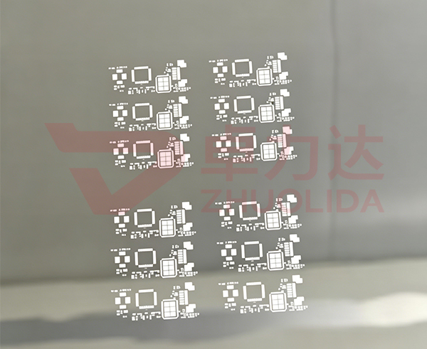
As the high-end manufacturing industry rapidly evolves toward miniaturization, high precision, and high consistency, the shortcomings of traditional mechanical cutting, laser processing, and conventional etching processes have become increasingly apparent in the production of micron-scale components. These methods are prone to causing issues such as stress-induced deformation of workpieces, rough edges, microstructural damage, and excessive dimensional tolerances, making them unable to meet the ultra-high-precision assembly requirements of fields such as precision instruments, semiconductors, smart sensors, and avionics. Precision Electroforming microfabrication, based on the principle of electrochemical ion-directed deposition, is a non-contact additive manufacturing technology capable of precisely replicating various ultra-fine patterns, high-density microporous arrays, and ultra-thin, irregularly shaped microcomponents. The finished products feature dense grain structures, are free of residual stress, and exhibit stable dimensional accuracy, making it the core advanced process for the fabrication of micro- and nano-scale metal components today. The Precision Electroforming Microfabrication Plant leverages ultra-clean, temperature-controlled, standardized production lines to establish a comprehensive microfabrication production system. This system supports the R&D of micro-part samples, small-batch customization, and large-scale mass production, effectively addressing industry pain points such as low yield rates, poor structural fidelity, and insufficient batch consistency associated with traditional microfabrication methods. The Precision Electroforming Microfabrication Company continues to deepen its expertise in the field of micro- and nano-electroforming, constantly optimizing electrolyte formulations, pulse deposition parameters, and microstructure compensation processes. By overcoming challenges such as uneven deposition, pattern distortion, and thin-wall deformation during microfabrication, the company provides core process support for China’s high-end precision manufacturing industry.
Precision electroforming microfabrication imposes extremely stringent requirements on the production environment, equipment precision, and process control standards. The entire process must be completed in a closed-loop system within a Class 100 cleanroom that is temperature-controlled and light-shielded, encompassing nine core processes: microstructure simulation and modeling, precision master mold fabrication, ultra-clean substrate activation, photolithographic micro-pattern transfer, uniform conductive layer plating, pulsed micro-electroforming deposition, non-destructive demolding and separation, stress relief annealing and modification, and micron-level precision quality inspection and packaging. Throughout the production process, the circulation rate of chemical solutions, deposition temperature, and pulse current density are controlled in real time to precisely regulate the growth rate of metal ions, thereby avoiding common microfabrication defects such as microporous blockage, thin-wall warping, grain porosity, and pattern misalignment. Precision electroforming microfabrication is compatible with a wide range of materials, including nickel alloys, copper, stainless steel, and specialty alloys. It can reliably process various precision microcomponents with micrometer-level thicknesses and micrometer-level aperture sizes, meeting the production needs for micro-parts across multiple fields. Precision electroforming microfabrication facilities categorize processing standards into three levels—civilian precision grade, industrial control grade, and high-end aerospace grade—based on the components’ intended applications, and adjust microdeposition compensation and surface protection processes accordingly. Precision electroforming microfabrication companies have established dedicated process databases for microelectroforming, standardizing processing parameters for components with different microstructures and materials. This enables rapid product iteration and ensures a high degree of consistency in the quality of mass-produced microcomponents.
Microstructural simulation modeling and the precision fabrication of master molds are the core preliminary processes for ensuring the accuracy of precision electroforming microfabrication. Given the characteristics of various microcomponents—including their minute dimensions, intricate structures, and high assembly precision—we use 3D simulation modeling to calculate metal ion deposition patterns and global stress distributions. This allows us to optimize the layout of micro-holes, micro-grooves, and irregular microstructures, compensate in advance for micro-machining side-etching errors, and prevent issues such as component deformation, assembly misalignment, and structural failure at the design stage. Specialized substrates with high flatness, high stability, and low thermal expansion are carefully selected for the fabrication of electroforming master molds. These undergo ultra-precision leveling, multi-stage degreasing, and plasma activation treatments to thoroughly remove trace amounts of oil, dust, and oxidized impurities from the surface, ensuring the master mold’s surface is exceptionally clean and flat—laying a solid foundation for the precise transfer of micro-patterns and uniform metal deposition. Precision electroforming microfabrication, optimized through upfront simulation, significantly enhances the structural fidelity and on-machine compatibility of microcomponents. Precision electroforming microfabrication facilities employ high-precision master mold fabrication processes to eliminate batch defects in microcomponents caused by master mold imperfections. Precision electroforming microfabrication companies keep pace with the evolution of micro- and nano-manufacturing technologies, continuously adapting to meet custom processing demands for ultra-fine, high-density, and complex, irregularly shaped microcomponents.
Ultra-clean photolithographic micro-pattern transfer and conductive activation processes directly determine the microstructure replication accuracy of precision electroforming microfabrication. Ultra-thin photoresist is uniformly coated and cured at a constant temperature in a light-shielded, ultra-clean workstation. Leveraging high-precision laser direct-writing alignment equipment, the process precisely replicates micron-scale micro-pore arrays, fine conductive patterns, micro-positioning structures, and irregular openwork micro-patterns. For composite microstructures with uneven density distribution, we employ zone-specific dynamic exposure and development technology to balance development rates across different areas, thoroughly eliminating defects such as jagged edges, misalignment, and missing features in the micro-patterns, thereby forming well-defined insulation protection zones and electroforming zones. Subsequently, a uniform, ultra-thin conductive film is deposited in the forming areas to ensure uniform adhesion and growth of metal ions, thereby preventing issues such as localized deposition discontinuities, uneven thickness, and missing microstructures. This enables the stable, integrated formation of micrometer-level precision structures, far exceeding the forming limits of traditional microfabrication processes. Precision electroforming microfabrication strictly minimizes pattern alignment errors, ensuring precise and uniform dimensions for every microstructure. Precision electroforming microfabrication facilities implement standardized control over lithography and conductive coating processes to eliminate accuracy deviations caused by human error. Precision electroforming microfabrication companies continuously iterate on high-definition micro-lithography systems to enhance the forming accuracy and stability of complex microcomponents.
Segmented pulse microelectroforming is the core forming process in precision electroforming microfabrication. The prepared master mold is placed in a sealed, temperature-controlled electroforming tank. A specialized low-stress electrolyte is selected to match the material of the component, and the pulse current, tank temperature, and electrolyte circulation and filtration rates are dynamically controlled. Using a layered, intermittent pulse deposition process, metal grains are allowed to grow and stack slowly, densely, and uniformly. This process involves no mechanical extrusion or high-temperature thermal damage, completely eliminating secondary processing stresses in microcomponents. The resulting micro-parts feature vertical, smooth side walls; uniform, open microporosity; and are free of burrs and deformation, with excellent mechanical properties and structural stability. Additionally, it enables the integrated formation of multiple complex microstructures in a single step, eliminating the need for secondary finishing and significantly reducing the production cycle of micro-parts, thereby meeting the demands of high-precision microcomponent mass production. Precision electroforming microfabrication allows for precise control of micrometer-level thickness and aperture parameters, fully meeting the processing standards for microcomponents in various high-end equipment. Precision electroforming microfabrication facilities are equipped with multi-stage chemical solution recirculation and purification systems to maintain stable solution activity and ensure consistent deposition results for batch production. Precision electroforming microfabrication companies continuously optimize pulse deposition parameters to effectively address industry challenges such as warping and grain porosity in thin-walled microcomponents.
Non-destructive demolding, stress optimization, and micron-level quality inspection are the critical final processes for enhancing the service performance of precision electroforming microcomponents. Once metal deposition meets specifications, a low-temperature, gentle, and non-destructive demolding process is employed to smoothly separate the microcomponents from the master mold, thereby preventing microstructural stretching, breakage, and deformation caused by forceful demolding. Following demolding, vacuum isothermal annealing is performed to completely eliminate residual deposition stresses within the components, thereby enhancing their structural strength, resistance to deformation, and dimensional stability. Subsequently, ultrasonic ultra-clean washing, mirror-finish micro-polishing, and anti-corrosion passivation and modification are carried out to remove trace impurities from the surface and improve the surface finish and weather resistance of the micro-components. Finally, 3D profilometers and laser micrometer measuring instruments are used to perform comprehensive dimensional accuracy verification, strictly controlling core metrics such as micro-hole aperture, pattern width, and panel flatness. Qualified products undergo anti-static vacuum packaging. Precision electroforming microfabrication establishes a full-process traceability and quality control system, strictly adhering to high-end microfabrication acceptance standards. The precision electroforming microfabrication facility implements a batch-by-batch sampling inspection system to strictly control the precision consistency of batch-produced products. The company meticulously manages the entire post-processing workflow to comprehensively ensure the quality of high-end microcomponents upon shipment.
Leveraging its core advantages of high precision, stress-free processing, and high fidelity, precision electroforming microfabrication is widely applied in three high-end fields: micro-components for precision instruments, semiconductor micro-components, and micro-parts for smart sensors. The precision electroforming microfabrication plant relies on standardized microfabrication processes to continuously improve the precision and yield of mass-produced micro-components. The precision electroforming microfabrication company is deeply committed to the micro- and nano-precision manufacturing sector, continuously refining the domestic precision electroforming microfabrication technology system.
Precision Instrument Microcomponents: Optical testing instruments, internal micro-filters for precision analytical equipment, grating microstructures, and positioning micro-components all demand extremely high dimensional accuracy and structural uniformity. Precision electroforming microfabrication ensures accurate microstructure reproduction and uniform pore sizes, guaranteeing stable and precise instrument measurement data. Precision electroforming microfabrication facilities operate in cleanroom environments, leaving no impurity residues, and are suited for the demanding operating conditions of precision instruments. Precision electroforming microfabrication companies employ meticulous parameter control to meet micron-level processing standards for high-end instruments.
Semiconductor Microcomponents Sector: Semiconductor packaging, conductive microplates for microcircuits, isolation microcomponents, and breathable micro-porous components require high precision, stable impedance, and freedom from dust contamination. Precision electroforming microfabrication ensures flat, clean surfaces and stable electrical conductivity, making it suitable for precision semiconductor packaging applications. Precision electroforming microfabrication facilities operate under a fully closed-loop production process, eliminating micro-particle contamination and ensuring high yield rates for semiconductor products. Precision electroforming microfabrication companies optimize low-stress forming processes to prevent deformation and failure of microcomponents during long-term use.
Smart Sensing Microcomponents: Industrial sensors, internal sensing microstructures in micro-detection devices, flow-guiding thin plates, and signal-transmission microcomponents require structural stability, fatigue resistance, and long-term precision. Precision electroforming microfabrication employs stress-free forming, offering excellent resistance to vibration and temperature fluctuations. Precision electroforming microfabrication facilities ensure high consistency in batch production, making them suitable for the mass production of sensing equipment. Precision electroforming microfabrication companies continuously iterate their processes to keep pace with the trend toward miniaturization in smart devices.
In summary, precision electroforming microfabrication has overcome the precision and structural limitations of traditional microfabrication processes and is one of the core technologies in modern micro- and nano-manufacturing. Precision electroforming microfabrication facilities rely on standardized and refined electrochemical additive manufacturing processes to achieve stable, high-precision mass production of miniature metal components. Precision electroforming microfabrication companies focus on the needs of high-end industries such as semiconductors, precision instruments, and smart sensors, continuously optimizing core precision electroforming microfabrication technologies to support the high-quality development of China’s micro-precision manufacturing industry toward high-end, refined, and self-reliant production.
Contact:赖先生
Phone:+86 18938693450
Tel:0755-2708-8292
Email:yw9@zldsmt.com
Add:深圳市宝安区福永镇新和村福园一路华发工业园A3栋
 Zhuolida