Welcome: Shenzhen Zhuolida Electronics Co.TD
Language:
 ∷
∷

∷
∷
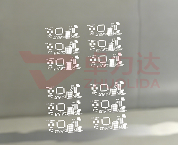
Metal electroforming is a specialized manufacturing technology that utilizes the principles of electrochemical deposition to achieve precision additive manufacturing of metals. Unlike traditional stamping, etching, and laser cutting processes, it offers distinct advantages such as the absence of mechanical stress, high forming accuracy, excellent micro-pore perpendicularity, and strong structural consistency. It is widely applicable to the production of ultra-thin metal components, high-density micro-pore arrays, precision mold cavities, and micro-scale functional devices. Against the backdrop of rapid technological evolution in the high-end semiconductor, new energy, precision industrial control, and optoelectronic instrument industries, the limitations of traditional machining—such as deformation, burrs, and precision constraints—have become increasingly apparent. Precision Electroforming, however, can effectively address these industry shortcomings. Metal electroforming relies on the uniform deposition and layering of metal ions to form structures. The entire process involves no external force contact and no high-temperature thermal damage, enabling the stable mass production of complex structures at the micrometer level. It is currently the core forming solution for high-end precision metal components. Metal Electroforming processing relies on dust-free, temperature-controlled, closed-loop production lines that cover the entire process chain—from master mold preparation, substrate pretreatment, pulse electroplating, non-destructive demolding, clean surface modification, to precision quality inspection—and can meet diverse production needs ranging from new product prototyping and small-batch customization to large-scale mass production. Manufacturers of metal electroforming continuously refine electrolyte formulations, pulse deposition parameters, and flatness compensation processes to address industry challenges such as warping in ultra-thin workpieces, side etching of micro-pores, color variations in batches, and dimensional deviations, thereby providing stable process support for high-end precision manufacturing across various fields.
The complete precision metal electroforming production process must be carried out in a Class 100 temperature-controlled, light-shielded, dust-free cleanroom. It is divided into nine core stages: process simulation modeling, selection and pretreatment of conductive substrates, laser lithography master mold fabrication, segmented pulse electroforming deposition, gentle and non-destructive demolding, multi-stage ultra-clean washing, functional coating modification, comprehensive precision inspection, and vacuum dust-proof encapsulation. Throughout the process, strict control is maintained over electrolyte temperature, pulse current density, deposition rate, and workshop cleanliness to prevent processing defects such as board warping, microporous blockage, rough inner walls, and residual stress. Metal electroforming is suitable for shaping a wide range of products, including pure nickel, nickel-cobalt alloys, ultra-thin metal foils, and high-density microporous templates, covering multiple application fields such as semiconductor packaging and testing, new energy filtration, precision optoelectronics, and industrial control sensors. Metal electroforming processes are organized into three tiers of process standards: general-purpose civilian grade, industrial precision grade, and high-end high-reliability grade. Deposition thickness, stress parameters, and surface protection processes are adjusted according to different usage scenarios to ensure workpieces are suitable for various complex operating conditions. Metal Electroforming manufacturers have established standardized process databases to document production parameters for workpieces of different thicknesses and structures, enabling rapid product revisions and consistent quality replication, thereby significantly improving the mass production yield of precision components.
Operating condition simulation modeling and master mold design are the core preliminary processes that ensure the accuracy and stability of metal electroforming. Technical personnel conduct 3D simulations based on the workpiece’s structural dimensions, array layout, operating temperature differentials, and equipment assembly benchmarks. They precisely calculate metal deposition compensation and global stress distribution, and optimally arrange functional micropores, positioning references, clearance grooves, and stress-relief structures to proactively mitigate issues such as poor assembly fit, fluid blockages, and structural deformation during mass production. For complex structures featuring large panel areas, high density, and ultra-fine pitch, a zoned deposition compensation design is employed to balance the difference in deposition rates between the center and edges of the panel, thereby resolving the industry-wide challenge of uneven thickness across the entire surface. After the drawings undergo a four-fold verification process covering dimensional accuracy, mechanical stability, temperature-induced deformation resistance, and assembly fit, the final master mold machining plan is finalized. Through upfront simulation and debugging, the metal electroforming process significantly improves workpiece machine compatibility and end-product yield rates. Metal electroforming manufacturers keep pace with industry trends toward miniaturization, array-based designs, and high reliability in precision components, continuously optimizing master mold design logic to rapidly adapt to the R&D and mass production needs of various new precision components.
The selection of conductive substrates and ultra-clean pretreatment lay a solid foundation for the quality of metal electroforming. During production, high-quality substrate materials with excellent flatness, uniform conductivity, and low residual stress are prioritized. Upon arrival, each substrate is individually screened for thickness tolerance, surface finish, and oxidation status, and any non-conforming substrates with scratches, deformation, or uneven conductivity are rejected. The pretreatment process sequentially includes ultrasonic degreasing, multi-stage ultra-pure water rinsing, constant-temperature drying, and plasma activation and leveling. This thoroughly removes oil, dust, and oxide layers from the substrate surface, enhances the adhesion of the photoresist dry film, and eliminates subsequent process defects such as photoresist delamination, localized etching, and pattern defects. For ultra-thin substrates thinner than 0.05 mm, an additional stress-relief aging treatment is performed to fully release the substrate’s inherent stress, thereby preventing warping and deformation of the finished product at the source. Metal electroforming strictly adheres to high-cleanliness production standards. High-end precision workpieces undergo a dual-activation process to ensure the utmost cleanliness of the panel surface. Metal electroforming manufacturers have optimized the pre-treatment processes on their production lines to achieve standardized and refined substrate processing, providing a reliable foundation for high-precision electroforming.
Laser lithography for pattern transfer and curing determines the structural replication accuracy of metal electroforming. The automatic application of photosensitive dry film and constant-temperature curing are performed in light-shielded, dust-free workstations. Leveraging high-precision laser direct-write alignment equipment, complex structures such as micro-hole arrays, irregular contours, precision patterns, and positioning holes are precisely replicated. For composite patterns with varying densities, zone-specific dynamic exposure technology is employed to balance the development rates across different areas, effectively eliminating defects such as pattern misalignment, jagged edges, and localized defects. Upon completion of development, a uniform and dense protective resin layer is formed. The masked areas prevent metal ion deposition, while the exposed areas serve as channels for the formed structures. This process reliably achieves integrated molding of micron-level precision structures, overcoming the limitations of traditional machining, which cannot produce ultra-fine micropores or ultra-thin irregular structures. Metal electroforming enables high-precision, uniform replication of structures across the entire surface, with dimensional errors strictly controlled within high-end industrial tolerance limits. Metal electroforming manufacturers are continuously upgrading their high-definition vision alignment systems to improve the consistency of large-format workpiece forming and meet the demands of large-scale precision production.
Segmented constant-temperature pulse electroforming is the core forming process in metal electroforming. The prepared master mold is placed in a sealed, temperature-controlled electroforming tank. Using a specialized, low-stress, eco-friendly electrolyte, the pulse current, tank temperature, and circulation/filtration rate are dynamically regulated. Through a layered, intermittent deposition process, metal grains are allowed to grow and stack uniformly, precisely controlling the workpiece thickness, micro-pore perpendicularity, and inner wall finish. The resulting metal components are free of side erosion, burrs, and microscopic scratches. Since the entire process involves no mechanical extrusion or high-temperature processing, there are no secondary internal stresses. These components are resistant to deformation and cracking under long-term high- and low-temperature conditions as well as vibration, making them ideally suited for the formation of ultra-thin, large-sized, and high-density precision workpieces. This process enables the simultaneous formation of multiple structures in a single step, streamlining secondary processing steps and effectively shortening the production cycle. Thanks to its stable deposition process, metal electroforming achieves a high degree of uniformity in the dimensions, performance, and appearance of mass-produced workpieces. Metal electroforming manufacturers have established an electrolyte circulation, filtration, and regeneration system that balances forming precision, mass production capacity, and environmental standards, enabling efficient and stable mass production.
Non-destructive demolding, clean surface modification, and precision quality inspection enhance the comprehensive performance of metal electroforming products. After electroforming deposition is complete, a low-temperature, gentle peeling process is used to separate the finished product from the master mold, eliminating structural damage and microporous collapse caused by forceful pulling. Subsequently, targeted ultrasonic cleaning, multi-stage purified water rinsing, and vacuum drying are performed to thoroughly remove residual chemicals and metal debris from the internal structure. Depending on the workpiece’s application scenario, anti-static, wear-resistant, and anti-corrosion passivation treatments are applied to enhance the workpiece’s service life and suitability for specific operating conditions. Finally, comprehensive quality inspections are conducted using 3D profilometers, laser dimension measuring instruments, and flatness testers to eliminate defective products. Qualified products are vacuum-sealed in anti-static packaging to isolate them from moisture and dust and prevent oxidative damage. The metal electroforming process establishes a full-process traceability and quality control system, with each step verified against high-end industry standards. Metal electroforming manufacturers exercise meticulous control over every post-processing step to ensure that finished products meet both precision and performance standards upon shipment.
Thanks to its core advantages of high precision, stress-free construction, and high consistency, metal electroforming is widely used in three major fields: semiconductor packaging and testing stencils, precision filtration components for new energy applications, and micro-components for optoelectronic instruments. Metal electroforming processes continue to evolve to meet the demands of high-end manufacturing, and manufacturers in this field are deeply committed to the precision electroforming sector, continuously refining the domestic precision forming process system.
Application Case: Semiconductor Packaging and Testing Templates—For chip ball placement and packaging printing templates, requirements for vertical micro-holes, a flat surface, and the absence of stress-induced deformation directly determine chip packaging yield. Metal electroforming enables the one-piece molding of high-density micro-hole arrays with smooth, taper-free inner walls, ensuring ball placement and printing without bridging and with minimal solder defects. Metal electroforming processes feature micrometer-level precision control, meeting the ultra-fine pitch packaging requirements of high-end chips. Metal electroforming manufacturers have optimized low-stress deposition processes to ensure stencils remain distortion-free even after long-term, repeated use.
Application Case: Precision Filtration Components for New Energy: Metal filter screens for energy storage and hydrogen energy equipment must be corrosion-resistant, have uniform pore sizes, and offer long wear life to withstand long-term fluid filtration conditions. Metal electroforming-produced filter screens feature uniform pore sizes, excellent permeability, and no localized defects, ensuring stable filtration precision. The metal electroforming process incorporates enhanced anti-corrosion and wear-resistant modifications to withstand complex acidic and alkaline environments. Manufacturers have optimized alloy composition processes to significantly extend the service life of the filter screens.
Application Case: Micro-Components for Optoelectronic Instruments: Microstructural components inside precision optoelectronic sensors and testing instruments demand extremely high standards for dimensional accuracy, flatness, and stability. Metal electroforming enables stress-free forming, ensuring precise structural alignment with equipment assembly standards and eliminating stray light interference. The entire metal electroforming process is conducted in a dust-free environment, leaving no impurity residues and guaranteeing the instrument’s measurement accuracy. Manufacturers of metal electroformed components fine-tune process parameters to meet the high-precision operational standards of optoelectronic equipment.
Overall, metal electroforming is currently the core advanced process for manufacturing high-end precision metal micro-components, completely overcoming the accuracy and deformation limitations of traditional machining. Relying on standardized, finely controlled closed-loop processes, metal electroforming enables high-precision, highly reliable, and high-yield mass production. Manufacturers specializing in metal electroforming focus on the needs of the semiconductor, new energy, and high-end optoelectronic industries, continuously optimizing core electroforming processes to help upgrade the quality of China’s precision manufacturing industry and drive the localization, refinement, and high-end development of high-end metal components.
Contact:赖先生
Phone:+86 18938693450
Tel:0755-2708-8292
Email:yw9@zldsmt.com
Add:深圳市宝安区福永镇新和村福园一路华发工业园A3栋
 Zhuolida