Welcome: Shenzhen Zhuolida Electronics Co.TD
Language:
 ∷
∷

∷
∷
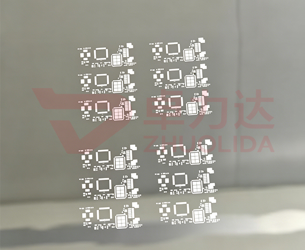
As the core hub for integrated circuits, new energy, medical precision equipment, and optoelectronic display industries in the Guangdong-Hong Kong-Macao Greater Bay Area, Shenzhen fully covers the entire industry chain of chip design, wafer packaging and testing, lithium battery energy storage, and minimally invasive devices. The market demand for various micron-level ultra-thin metal microstructures, high-density microvia arrays, and three-dimensional precision components continues to surge. Traditional stamping, laser cutting, and chemical etching processing of ultra-thin metal parts generally suffer from shortcomings such as high internal stress in the sheet, pronounced taper on microvia sidewalls, short wear cycle life, and poor dimensional consistency in large-panel arrays, making them unable to meet advanced packaging, medical implantation, energy storage filtration, and other high-precision mass production standards. Shenzhen electroforming machining relies on pulse electrochemical layer-by-layer metal deposition additive forming principles, with no mechanical external pressure or high-temperature thermal burns throughout the process. It can integrally form vertical smooth microvias, three-dimensional microchannels, ultra-thin shaped thin sheets, and high-precision printed templates. Dimensional replication accuracy reaches submicron level, and wear and corrosion resistance far surpasses traditional processing techniques. It is the mainstream local high-end precision metal component forming solution in Shenzhen. Shenzhen electroforming processing integrates master mold lithography preparation, constant temperature pulse electrodeposition, gentle and non-destructive demolding, semiconductor-grade clean functional modification, multi-condition simulation detection, integrated Class 100 light-avoidance, dust-free closed-loop production line, while also supporting cutting-edge chip R&D with small-batch samples, continuous large-scale support for new energy and medical equipment, and adapting to the customized production needs of semiconductors, energy storage, minimally invasive medical, and optoelectronic display categories. Shenzhen Electroforming manufacturers are rooted in Shenzhen's complete electronics manufacturing supply chain, relying on local industry-university-research precision machining technology resources. They continuously optimize core processes such as low-stress nickel amino sulfonate electrolyte, dynamic pulse balanced deposition, and large-area flatness compensation, tackling industry pain points such as ultra-thin workpiece warping, ultra-microhole inner wall roughness, and cross-batch dimensional deviations. They have established a hierarchical Precision Electroforming production control system to support quality improvement, efficiency improvement, and domestic substitution of high-end precision manufacturing industries in the Greater Bay Area.
The entire standardized production process is carried out in a closed-loop Class 100 constant temperature light-avoidance dust-free workshop, divided into nine core processes: downstream product working condition simulation master mold design, high-flatness conductive substrate selection dust-free pretreatment, LDI laser high-precision lithography master mold pattern creation, segmented constant temperature pulse electroforming electroforming deposition, gentle and non-destructive layered demolding, multi-stage ultra-clean microporous deep purification, stress aging and wear-resistant anti-static composite coating, multi-environment benchmarking comprehensive testing, and anti-static light-shield vacuum sealed encapsulation. Throughout the process, the electrolyte temperature is strictly controlled, pulse current density, metal deposition thickness, and workshop dust particle concentration, with a focus on avoiding four major critical precision processing defects: workpiece surface warping, microhole taper shift, inner wall metal burrs, and surface static residual residue. Shenzhen electroforming processing is divided into three main categories: semiconductor wafer ball placement templates, new energy lithium battery/fuel cell precision nickel mesh filters, and MicroPort medical ultra-thin microstructural components, adapting to differentiated precision component production conditions for AI computing chips, energy storage stacks, and endoscope implant devices. Shenzhen electroforming processing is divided into three levels of independent process control standards: consumer electronics grade, new energy industry high-frequency grade, and semiconductor/medical high-reliability grade, with differentiated adjustments to electroforming deposition rate, surface coating formulas, and thermal cycling aging verification processes. Shenzhen electroforming manufacturers have built dedicated process databases for multiple specifications and materials, matching dedicated electroforming parameters for ultra-thin plates under 0.03mm, ultra-large 12-inch whole panels, and ultra-fine pitch high-density array workpieces, ensuring highly unified and stable flatness, aperture, and wear and corrosion resistance of workpieces in the same batch and across batches.
Downstream end-product working condition simulation and master mold graphic structure design are core processes before Shenzhen electroforming machining is put into production. Technical staff conduct 3D simulation modeling based on workpiece dimensions, microstructure array layout, standard microhole diameters, high and low temperature cycling temperature differences, and positioning references for local Shenzhen automated packaging and assembly equipment. They accurately calculate electroforming metal deposition compensation and large-scale stress distribution, integrate functional microvias, equipment positioning reference holes, workpiece limit avoidance slots, and edge stress release trenches to proactively avoid mass production defects such as workpiece bonding and assembly extrusion deformation, microvia blockage during long-term use, electrostatic breakdown of precision chips, and stray light interference with optoelectronic sensing components. For the 12-inch HBM high-bandwidth storage of ultra-large electroforming ball planting templates, a distributed thickness dynamic compensation structure was added to balance the thickness differences between the center and edge areas of the panel surface. After four layers of verification—forming dimensional accuracy, mechanical cycle durability, anti-static insulation, and wide temperature deformation resistance—the master mold machining plan was locked. Shenzhen electroforming machining completed simulation and debugging of extreme high and low temperatures and continuous vibration conditions in advance, greatly improving the first-time adaptation rate of workpieces and the overall yield rate of downstream end products. Shenzhen electroforming manufacturers keep pace with the iteration pace of fan-out fan-out packaging, solid-state batteries, and minimally invasive interventional devices, quickly completing various new model redesigns, debugging, and mass production and delivery.
High-flatness conductive substrate selection and ultra-clean panel surface pretreatment lay a solid foundation for submicron-level forming accuracy in Shenzhen electroforming processing. Production uses low-roughness, uniformly conductive, low-inherent stress special quartz and metal substrates as master mold carriers. Each piece is stored to screen substrate thickness tolerances, surface density smoothness, and primary oxidation defects, removing surface scratches, excessive internal stress, and uneven conductivity, ensuring uniform photoresist coating and electroforming layer deposition from the source. The pretreatment process sequentially completes four standardized steps: alkaline dust-free ultrasonic degreasing, multi-stage closed-loop ultrapure water circulation rinsing, plasma interface activation, and micro-etching leveling of the panel, thoroughly removing substrate rolling oil stains, primary oxide layers, and ultrafine dust impurities, greatly improving uniform adhesion of subsequent photosensitive dry films and eliminating delamination and pattern defects in high-density micropore array areas; For ultra-thin substrates below 0.05mm thick, an additional temperature-controlled stress relief aging process is added to fully release the panel's inherent internal stress. Shenzhen electroforming processing strictly enforces ultra-high cleanliness control standards for semiconductors and medical components, isolating micron-level dust particles throughout the process to prevent impurities embedded in the electroforming layer causing microporous blockages, chip circuits, and medical device contamination. Shenzhen electroforming manufacturers have graded and refined pretreatment operation procedures, performing dual plasma activation deep purification processes for automotive-grade semiconductors and implantable medical supporting electroforming workpieces.
LDI laser high-precision lithography master mold pattern transfer controls core accuracy in Shenzhen electroforming micro-hole array replication. The sealed, low-light, Class 100 dust-free workstation completes ultra-thin photosensitive dry film uniform thermal pressing and curing, equipped with high-precision laser direct writing vision alignment equipment to simultaneously and accurately expose functional microvias, equipment positioning holes, and microchannel three-dimensional pattern patterns in one go. For composite array patterns with significant density differences, a segmented dynamic exposure energy adjustment process is used to balance the development speed between dense microporous areas and blank border areas, effectively eliminating pattern jaggedness, hole position shift, and local adhesive deficiency defects. After constant temperature slow and uniform development, a complete photoresist protective master mold is formed. The adhesive layer blocks metal ion deposition, and the exposed area is the electroformed microporous channel, allowing complete submicron-level replication of all structural parameters. Shenzhen electroforming processing can achieve synchronous and uniform forming of tens of thousands of array micro-vias, with all-domain aperture and hole spacing errors stably controlled within the micron tolerance range of Shenzhen's high-end semiconductor and medical manufacturing sectors. Shenzhen electroforming manufacturers continuously iterate their high-definition visual alignment systems, compressing dynamic graphic alignment errors to the micron range to meet the continuous usage needs of high-speed automated packaging and testing and medical assembly production lines in Nanshan and Bao'an.
Segmented pulse constant temperature electroforming deposition is the core forming process in Shenzhen electroforming processing. The conductive master mold completed by photolithography is immersed in a sealed constant temperature anti-corrosion electroforming tank, using low-stress nickel-cobalt alloy and high-purity nickel sulfonate special environmentally friendly electrolyte. The equipment system dynamically controls pulse current, constant temperature of the bath liquid, and multiple circulation filtration rates in real time. It employs segmented intermittent layered deposition technology to evenly stack dense metal grains, precisely controlling the overall thickness of the workpiece and the surface finish of the micro-hole inner wall. The final molded micro-hole inner wall is vertical without taper, no metal burrs, and no lateral corrosion defects. The entire forming process is electrochemical additive manufacturing, with no mechanical stamping or laser high-temperature thermal burns. The formed metal workpieces have no secondary processing stress and are not easily deformed under long-term high and low temperature cycling conditions. This process is perfectly suited for the integrated mass production of ultra-thin, large-sized precision components. Shenzhen electroforming processing can simultaneously complete integrated molding of functional microvias, limit avoidance slots, and positioning reference holes, streamlining secondary processing steps and shortening the overall production and delivery cycle. Shenzhen electroforming manufacturers have established multiple filtration and recycling systems for electrolytes, balancing micron-level forming precision, large-scale mass production capacity, and environmental protection control requirements in Shenzhen's regional industrial environment.
Gentle, non-destructive layered demolding and microhole cleaning modification optimize the long-term comprehensive performance of electroforming workpieces in Shenzhen. After electroforming metal deposition is completed, a low-temperature and mild peeling process is used to completely separate and form the metal electroformed parts from the photolithography master mold, preventing violent pulling that could cause microhole collapse or surface bending damage; After demolding, the workpieces are sent into a continuous multi-stage purification unit, where electrolyte residues and fine metal debris inside the micropores are thoroughly removed through microporous targeted ultrasonic unblocking, multi-stage high-purity water circulation washing, and vacuum low-temperature drying. In response to Shenzhen's local demand for semiconductor, energy storage, and medical wafer packaging and testing with electrostatic sensitivity and long-term cycle conditions of extreme high and low temperature aging, electrolytic polishing, anti-static passivation, and high-temperature wear-resistant composite coating treatments are simultaneously carried out, reducing the probability of solder paste and foreign matter adhesion on microporous inner walls and electrolyte solutions, suppressing static accumulation and penetrating precision chips and implanted devices, significantly improving the durability of repeated machine use of workpieces. Shenzhen electroforming processing can precisely adjust coating thickness and surface roughness as needed, adapting to three differentiated usage scenarios: semiconductor ball implantation printing, energy storage precision filtration, and minimally invasive medical micro-components. Shenzhen electroforming manufacturers integrate continuous processes such as electroforming forming, multi-stage cleaning, and surface coating, significantly shortening the overall delivery cycle for customized workpiece orders.
Comprehensive multi-environment monitoring and light-shielding vacuum packaging ensure the final quality control baseline of Shenzhen electroforming processing before shipment. The workshop is equipped with 3D profilometers, laser aperture detectors, high-precision flatness testers, electrostatic impedance testers, and thermal cycle simulation equipment to perform comprehensive and detailed inspections of workpiece dimensions, micro-hole diameter accuracy, board flatness, and anti-static insulation performance; Simultaneously replicates Nanshan Semiconductor's wide-temperature vibration, Pingshan energy storage equipment continuous steady-state operation, and Bright Medical's sterile simulation under real working conditions for on-site verification to precisely verify workpiece alignment accuracy, microvia smoothness, and long-term deformation stability. Qualified finished products undergo anti-static vacuum sealing at a light-protected Class 100 dust-free station, isolating light, moisture, and dust impurities during storage and transportation to prevent alloy plate oxidation, microporous blockage, and optical light-blocking performance. Shenzhen electroforming processing has established a full-process traceability quality inspection system for each item, strictly inspecting and retaining complete records against downstream semiconductor and medical industry original drawings. Automotive-grade and implantable medical high-end workpieces additionally retain a full set of environmental simulation test data. Shenzhen electroforming manufacturers fully retain pulse parameters, electrolyte ratios, and finished product inspection data for each batch, achieving stable and reproducible processes for the same workpiece and unified and controllable batch quality.
Shenzhen electroforming processing widely applies three core supporting scenarios in the Greater Bay Area: local AI computing power semiconductor ball placement templates, new energy storage precision nickel mesh filters, and MicroPort medical ultra-thin microstructural components. Shenzhen electroforming processing keeps pace with the development trends of precision manufacturing miniaturization, ultra-fine pitch, and high reliability industries, continuously iterating and optimizing complete electroforming processes. Shenzhen electroforming manufacturers are deeply cultivating core technologies for precision electroforming in the Pearl River Delta, continuously tackling difficulties in localizing high-end precision metal components, and helping Shenzhen and the Greater Bay Area semiconductor, new energy, and minimally invasive medical industries improve quality and efficiency.
AI computing semiconductor ball placement template application case: High-end GPU and memory chip pad arrangements at Shenzhen Nanshan and Lingang computing power bases are ultra-fine and dense, with strict requirements for template microvia verticality and overall array dimension consistency. Shenzhen electroforming processing has no taper-smooth inner wall microholes, solder paste demolding is smooth without bridging or solder defects, and wafer ball placement yield remains stable and high. Shenzhen electroforming processing optimizes large-area full-area dynamic thickness compensation process, with no local thickness deviations and long-term stable flatness. Shenzhen electroforming manufacturers have upgraded their all-domain balanced pulse electroforming system to meet the mass production needs of large-scale continuous ball placement for AI chips.
New energy energy storage precision filtration nickel mesh application cases: Shenzhen Pingshan, Longhua energy storage, hydrogen stack equipment electrolyte and hydrogen filter elements are frequently reused, filter screens are wear-resistant, microporous uniform, and have strict corrosion resistance indicators. Shenzhen electroforming machined nickel-cobalt alloys have dense electroforming layers with high hardness, ensuring no deformation or clogging after hundreds of thousands of fluid erosions, ensuring stable filtration accuracy. Shenzhen electroforming fabrication features a full-domain distributed stress release structure, ensuring long-term high-pressure working conditions with flat and stable panel surfaces without warping. Shenzhen electroforming manufacturers optimize anti-corrosion insulation composite coatings to meet large-scale plate supply orders for high-power energy storage stacks.
MicroPort Medical Ultra-thin Microstructural Component Application Case: Shenzhen Guangming Medical Device Industrial Park Endoscopes and implantable sensing thin sheets pursue ultra-thin, burr-free, biocompatible, and micron-level precision dimensions. Shenzhen electroforming processes 0.03–0.08mm one-piece thin-walled components, stress-free, no microscopic sharp edges, suitable for human implantation and minimally invasive procedures. Shenzhen electroforming processing produces a full Class 100 sterile and dust-free production process, with no metal impurity precipitation, meeting medical access cleanliness standards. Shenzhen electroforming manufacturer uses an exclusive medical-grade passivation modification process, withstanding repeated high-temperature sterilization and significantly extending the service life of medical devices.
Overall, Shenzhen electroforming processing is an indispensable core additive molding process for high-end precision components in semiconductors, new energy, and MicroPort medical care; Relying on pulse electrochemical additive forming processes, Shenzhen electroforming processing has completely overcome the inherent bottlenecks of traditional etching, stamping, and laser cutting in forming precision, wear life, and extreme temperature stability; Shenzhen electroforming manufacturers leverage the location advantages of Shenzhen's complete integrated circuit, new energy, and medical equipment industry clusters, continuously iterating the full set of high-reliability precision electroforming core processes, comprehensively empowering the high-quality domestic development of high-end precision manufacturing industries in the Guangdong-Hong Kong-Macao Greater Bay Area.
Contact:赖先生
Phone:+86 18938693450
Tel:0755-2708-8292
Email:yw9@zldsmt.com
Add:深圳市宝安区福永镇新和村福园一路华发工业园A3栋
 Zhuolida