Welcome: Shenzhen Zhuolida Electronics Co.TD
Language:
 ∷
∷

∷
∷

Product Overview
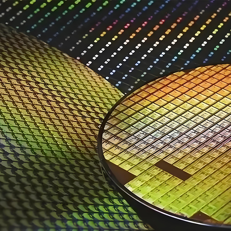
Electroformed ABF Substrate Balling Masks are core supporting components developed specifically for the balling process of ABF (Advanced Buffer Layer) chip substrates. Based on metal electroforming micro-nano processing technology, they serve as critical consumables in the semiconductor advanced packaging supply chain. Serving as the “bridge” connecting chips to substrates, the placement accuracy of ABF substrates directly determines chip electrical connection reliability and packaging yield. Electroformed ball placement masks provide precise positioning references for ABF substrate ball placement by accurately replicating nanoscale ball placement hole structures. Crafted from high-performance metals like nickel-cobalt alloys and high-purity nickel, this product delivers core advantages including precise hole positioning, smooth hole walls, chemical corrosion resistance, and zero mechanical deformation. It effectively addresses issues inherent in traditional masks—such as hole position deviation, edge burrs, and susceptibility to deformation—making it widely compatible with advanced packaging scenarios for high-end ABF chip carrier boards. This solution serves as a vital enabler for advancing chips toward higher density, miniaturization, and enhanced reliability.
Core Features
Nano-level Ball Placement Precision: Leveraging the integration of Precision Electroforming and photolithography technologies, ball placement hole diameter accuracy reaches ±0.1μm with positioning error ≤±0.05μm. Minimum hole diameter extends to 5μm, perfectly matching the ultra-fine pitch ball placement requirements of ABF substrates. This ensures zero deviation in ball placement, establishing a robust foundation for chip packaging.
Smooth, Burr-Free Wall Surfaces: The non-contact electroforming deposition process eliminates mechanical cutting damage, achieving a ball placement hole wall roughness of Ra ≤ 0.05μm. Free from burrs and flared deformation, it prevents defects like ball jamming, cold soldering, and bridging during placement, thereby enhancing yield rates.
High stability with no deformation: Constructed from high-purity nickel or nickel-cobalt alloy, it offers excellent mechanical strength and stability with flatness ≤0.01mm. It withstands prolonged exposure to high temperatures and flux corrosion during ball placement without deformation or warping, ensuring ABF substrate ball placement meets alignment standards.
Superior Chemical Corrosion Resistance: Specially treated materials withstand exposure to multiple chemical agents including flux, cleaning agents, and etching solutions during ball placement. Corrosion resistance testing exceeds 1000 hours, with a service life of over 800 ball placement cycles, significantly reducing packaging consumable costs.
High-Density Adaptability: Supports high-density layouts with hole densities ≥2000 holes/mm². Customizable ball placement hole dimensions, spacing, and layout based on ABF chip carrier models and pin counts. Compatible with mainstream advanced packaging processes like BGA, CSP, and FCBGA, flexibly meeting diverse packaging demands.
Practical Application Results
Significantly Improved Packaging Yield: ABF chip carriers equipped with electroformed ABF carrier ball placement masks achieve a first-pass ball placement yield exceeding 99.5%. This represents a 3%-5% improvement over traditional stamping/etching masks, effectively resolving high-frequency issues such as ball placement misalignment, cold solder joints, and bridging. Consequently, it reduces rework rates and cost losses in semiconductor packaging.
Enhanced Chip Electrical Stability: Precise ball placement and defect-free hole design ensure consistent connections between ABF substrates and chip pins, reducing contact resistance and signal transmission loss. Post-packaging chip conductivity improves by 2%, while signal transmission stability increases by 15%, meeting high-frequency and high-speed operational demands of premium chips.
Adaptation to high-density packaging demands: Perfectly supports ABF substrate ball placement for 1nm/3nm advanced process chips, enabling ultra-fine pitch (below 0.1mm) ball placement. This meets packaging trends toward denser chip pins and smaller form factors, facilitating the adoption of high-end ABF chip substrates in core products like mobile processors, AI chips, and server chips.
Optimized Packaging Efficiency and Cost: Enhanced compatibility with automated ball placement equipment increases process efficiency by 20% and extends stencil lifespan by 30%. This reduces packaging consumables cost per ABF chip carrier by 15% while minimizing equipment downtime for maintenance, thereby boosting overall packaging line productivity.
Adaptation to Complex Packaging Conditions: In high-temperature, high-humidity semiconductor packaging environments, the mask plate exhibits no deformation or corrosion failure. It reliably supports large-scale mass production scenarios, achieving ball placement consistency ≥99.8% for batch-produced ABF carrier boards. This meets the requirements for scalable and standardized semiconductor packaging.
Application Areas
High-End Consumer Electronics Chip Packaging: Supports ABF chip carriers for high-end consumer electronics such as smartphone AP chips, computer CPUs, and GPUs. Ensures packaging reliability through high-precision ball placement masks, enabling the high-performance and miniaturization of consumer electronics.
AI/Server Chip Packaging: ABF substrate packaging for AI training chips and data center server chips. Meets high-density, high-computing-power packaging demands, providing core support for AI computing power enhancement and server stability.
Automotive Electronics Chip Packaging: ABF substrates for in-vehicle autonomous driving chips and automotive-grade power chips. The high stability and corrosion resistance of ball placement masks meet the demanding packaging conditions of automotive electronics, including high temperatures and vibration resistance.
Communication Chip Packaging: ABF substrate packaging for 5G/6G communication chips and RF chips. Precise ball placement ensures stable signal transmission, supporting high-speed, low-loss communication requirements for telecommunication equipment.
Advanced Semiconductor Packaging Mass Production: Tailored for semiconductor packaging factories' large-scale ABF substrate ball placement production lines, providing high-consistency, high-durability electroforming ball placement mask support services to drive the scaled development of the advanced packaging industry.
Contact:赖先生
Phone:+86 18938693450
Tel:0755-2708-8292
Email:yw9@zldsmt.com
Add:深圳市宝安区福永镇新和村福园一路华发工业园A3栋

 Zhuolida