Welcome: Shenzhen Zhuolida Electronics Co.TD
Language:
 ∷
∷

∷
∷

Product Overview
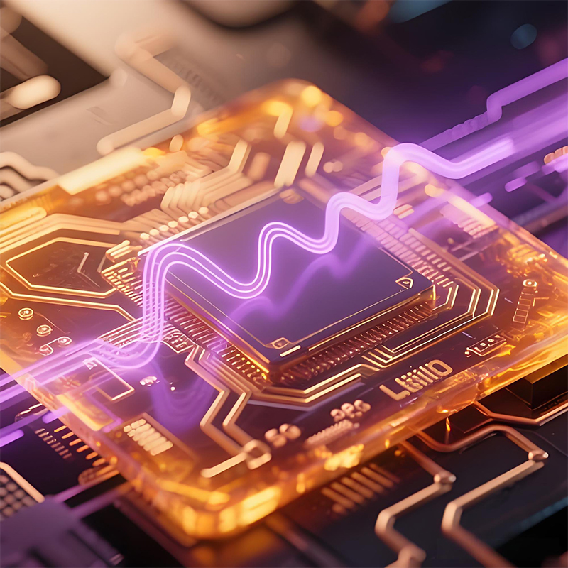
Wafer electroforming masks serve as core precision components throughout semiconductor chip manufacturing, packaging, and testing processes. Leveraging metal electroforming micro/nanofabrication techniques, these masks combine photolithography masks with metal electroplating to precisely replicate complex patterns ranging from nanometers to micrometers. They provide accurate pattern transfer references for critical wafer processes including lithography, etching, and ball bonding. Constructed from high-performance metals like nickel and nickel-cobalt alloys, this product delivers core advantages including exceptional pattern accuracy, freedom from mechanical stress, superior dimensional consistency, and chemical corrosion resistance. It effectively resolves industry pain points such as pattern distortion and edge burrs inherent in traditional mask fabrication. Widely applicable across semiconductor IC chip manufacturing, semiconductor sensors, MEMS devices, and optoelectronic components. It serves as a critical enabler for advancing semiconductor chips toward higher density, miniaturization, and precision, spanning the entire semiconductor industry lifecycle from R&D prototyping to mass production.
Core Features
1. Nanometer-level precision tailored for high-end semiconductor demands: Leveraging Precision Electroforming and deep ultraviolet lithography technology, line width accuracy reaches ±0.1μm with a minimum line width of 0.5μm. Pattern positioning accuracy of ±0.05μm perfectly meets the pattern transfer requirements for 1nm/3nm advanced process chips in the semiconductor industry, ensuring chip lithography precision.
2. Complex Pattern Formation for Diverse Chip Manufacturing: Enables one-step formation of intricate patterns including high-density lines, fine features, and irregular apertures. Pattern density ≥1000 lines/mm eliminates multi-step processing, accommodating design requirements for IC chips, MEMS devices, and other semiconductor products while preventing misalignment risks.
3. Stress-Free and Distortion-Free for Packaging Stability: Utilizes a non-contact metal deposition process with no mechanical cutting or heat-affected zones, fully preserving material properties. The mask plate flatness is ≤0.01mm, ensuring perfect alignment with the wafer during lithography and ball placement. This prevents pattern transfer distortion and enhances chip yield.
4. Chemical corrosion resistance for semiconductor environments: Utilizes corrosion-resistant metals that withstand exposure to photoresists, etchants, developers, and other chemicals in semiconductor manufacturing. Corrosion resistance tested for over 1000 hours, suitable for semiconductor fabs with controlled temperature/humidity and complex chemical environments.
5. High Consistency for Mass Production: Automated electroforming lines paired with AI vision inspection enable real-time monitoring of critical parameters like pattern dimensions and line widths. Batch production consistency reaches ≥99.8% with a yield rate of up to 99.7%, perfectly meeting the semiconductor industry's demands for large-scale, standardized mass production.
6. Flexible Customization for All-Scenario Applications: Supports customization for mainstream wafer sizes including 8-inch and 12-inch. Patterns, line widths, and thicknesses can be adjusted according to semiconductor product specifications to accommodate processes like lithography and packaging. Rapid prototyping within 24 hours meets both R&D and mass production needs.
Practical Application Results
1. Significant Improvement in Chip Lithography Yield: During IC chip lithography, the use of wafer electroforming masks achieves pattern transfer efficiency ≥99.9%, boosting chip lithography yield by 3%-5%. This effectively resolves chip scrap issues caused by pattern distortion and burrs in traditional masks, reduces chip manufacturing costs, and meets high-end chip mass production demands.
2. Semiconductor Device Precision Optimized: In MEMS and optoelectronic sensor manufacturing, precise micro/nano pattern replication enhances device sensitivity by over 15% and stability by 20%. This aligns with industry trends toward miniaturized, high-precision semiconductor sensors, serving applications in smart wearables and automotive electronics.
3. Dual Enhancement of Mass Production Efficiency and Capacity: Highly compatible with automated semiconductor lithography and packaging equipment, reducing debugging time and boosting production efficiency by over 20%. Simultaneously, mask plates achieve a lifespan exceeding 1,000 lithography cycles, minimizing consumable replacement frequency. This drives overall capacity growth in semiconductor production lines while lowering unit production costs.
4. Support for Advanced Process Chip Manufacturing: Perfectly enables pattern transfer for 1nm/3nm advanced process chips, achieving precise replication of fine lines and high-density patterns. This overcomes the precision limitations of traditional masks, helping the semiconductor industry break through advanced process technology bottlenecks and driving chips toward miniaturization and higher computing power.
5. Ensuring Semiconductor Product Consistency: Mass-produced masks exhibit exceptional dimensional and pattern consistency, guaranteeing uniform chip performance across all wafer batches. This eliminates performance fluctuations caused by mask variations, meeting the semiconductor industry's core demands for standardized, scalable production and enhancing product competitiveness in the market.
Application Fields
1. IC Chip Manufacturing: Core application in the lithography process for logic chips, memory chips, power chips, and other ICs. Serves as the essential masking component for pattern transfer, precisely replicating chip circuit patterns to support advanced process manufacturing for chips in mobile phones, computers, servers, and other end devices.
2. Semiconductor Sensor Field: Used in manufacturing MEMS gyroscopes, optoelectronic sensors, pressure sensors, and similar products. Through precise micro/nano pattern masks, it enables sensor miniaturization and high precision, supporting downstream semiconductor applications in automotive electronics, smart wearables, and industrial control.
3. MEMS Device Sector: Supports precision structural processing for MEMS accelerometers, microfluidic chips, and other MEMS devices. Leveraging complex pattern formation capabilities, it enhances device sensitivity and stability, driving the MEMS industry toward high-end development.
4. Semiconductor Packaging: Processes lead frame and bump masks for chip packaging, precisely controlling pattern dimensions to support mainstream BGA, QFP, and CSP packaging processes, thereby enhancing packaging accuracy and reliability.
5. Optoelectronic Devices: Manufacture of optoelectronic components including optical communication chips, laser chips, and display panel driver chips. High-precision pattern masks enable accurate formation of optical paths and circuits, enhancing device optoelectrical performance for applications in 5G communications and display industries.
Contact:赖先生
Phone:+86 18938693450
Tel:0755-2708-8292
Email:yw9@zldsmt.com
Add:深圳市宝安区福永镇新和村福园一路华发工业园A3栋

 Zhuolida