Welcome: Shenzhen Zhuolida Electronics Co.TD
Language:
 ∷
∷

∷
∷
We customize high-precision electroformed printing stencils adopting stress-free integrated photolithography electroforming technology with high-purity nickel-cobalt alloy. Featuring seamless integral structure, zero thermal deformation and no internal stress, our stencils have tapered mirror hole walls for clean demolding and ultra-low slurry residue, effectively solving solder paste bridging, cold solder and missing printing issues. With high printing accuracy, excellent consistency and superior wear resistance, custom stepped structures, special-shaped holes and ultra-fine pitch high-density arrays are available. Widely used in SMT mounting, semiconductor packaging, optoelectronic display, precision electronics and new energy vehicle electronics for high-speed automatic mass production. One-stop mold opening, processing and customization services are provided.
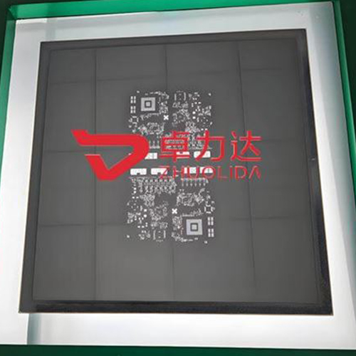
Electroformed printing stencils are high-precision integrated tooling molds manufactured from high-purity nickel-cobalt alloy via stress-free photolithography electroforming technology, serving core processes of SMT mounting, semiconductor packaging and precision printing. Eliminating defects of traditional laser-cut and etched stencils, the products feature zero internal stress, no thermal deformation and seamless integral structure. With micron-level precise array holes, smooth vertical walls and professional demolding taper, they fundamentally solve common printing problems such as solder paste residue, bridging, cold solder, missing printing and uneven thickness. Boasting high flatness, high hardness, excellent wear resistance and outstanding paste release performance, the stencils deliver superior batch consistency. Custom stepped holes, special-shaped holes and non-standard thicknesses are available. Widely applied in SMT printing, chip packaging, Mini LED and precision component mass production, they are essential high-precision molds for advanced electronic manufacturing.
Stress-Free Integrated Molding: Integrally formed by pure photolithography electroforming without stamping, laser thermal damage or etching corrosion. Zero internal stress prevents deformation, warpage and displacement during long-term high-speed printing, ensuring stable mass production.
Tapered Demolding Structure: Unique narrow-in and wide-out tapered hole design with mirror-smooth burr-free step-free walls enables smooth solder paste and slurry demolding with ultra-low residue, effectively reducing bridging, tailing and cold solder defects.
Ultra-High Aperture Consistency: Micron-level precise hole making ensures highly uniform full-panel aperture, pitch and shape with minimal thickness error, delivering far higher printing consistency for high-density arrays than traditional stencils.
High Hardness & Long Service Life: Nickel-cobalt alloy substrate features high hardness and toughness, resisting repeated wiping and high-frequency printing friction without hole expansion or wear, achieving a longer service life than laser and etched stencils.
Multi-Functional Customization: Custom stepped thickness, local thickening/thinning, special-shaped holes and special avoidance structures are available to meet diverse precision printing requirements for ultra-fine pitch processes.
Ultra-High Printing Precision: Precisely controlled aperture position tolerance with micron-level forming accuracy adapts to ultra-fine 0.2mm pitch, microchips and precision component printing, significantly improving production yield.
Excellent Paste Demolding Performance: Low-surface-energy smooth hole walls reduce paste adhesion for clean demolding and minimal residue, ensuring full and uniform printed patterns without material accumulation or clogging during continuous operation.
Extreme Structural Stability: Seamless integral structure with high flatness and uniform tension maintains stable performance during long-term mass production, avoiding printing offset and thickness deviation.
Fatigue & Wear Resistance: High-performance alloy resists friction and fatigue, tolerating tens of thousands of repeated printing, wiping and cleaning cycles with stable aperture size and no precision attenuation.
Powerful Process Adaptability: Compatible with solder paste, silver paste, conductive adhesive, insulating slurry and other materials. Fully adaptable to automatic high-speed printing equipment and various precision electronic mass production processes.
SMT Mounting Printing: Precision solder paste printing for PCB circuit boards, micro resistors, capacitors and precision components, eliminating printing defects of fine-pitch devices.
Semiconductor Packaging: Applied in BGA, QFN, Chiplet and wafer-level packaging ball mounting and printing processes for high-end precision chip mass production.
Optoelectronic Display Industry: Slurry printing and precision coating for Mini LED and Micro LED lamp boards to ensure uniform and consistent display circuits.
Precision Electronic Components: Conductive slurry printing for sensors, radio frequency components, precision inductors and capacitors to realize high-precision circuit forming.
New Energy Electronics: Precision printing processes for power battery accessories, energy storage electronic components and vehicle-mounted electronic slurries.
Industrial Control Equipment: High-precision circuit printing and forming for industrial control boards, high-frequency precision circuit boards and medical electronic circuits.
Contact:赖先生
Phone:+86 18938693450
Tel:0755-2708-8292
Email:yw9@zldsmt.com
Add:深圳市宝安区福永镇新和村福园一路华发工业园A3栋
 Zhuolida