Welcome: Shenzhen Zhuolida Electronics Co.TD
Language:
 ∷
∷

∷
∷
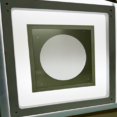
Electroformed wafer templates are ultra-precision electroforming molds developed for semiconductor wafer processes, integrally fabricated from high-purity nickel-cobalt alloy via photolithography electroforming technology, compatible with 8-inch and 12-inch wafer manufacturing procedures. Free of mechanical cutting and laser thermal stress, the flat templates feature distortion-free surfaces.
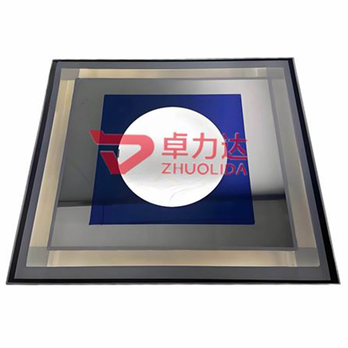
Electroformed wafer templates are ultra-Precision Electroforming molds developed for semiconductor wafer processes, integrally fabricated from high-purity nickel-cobalt alloy via photolithography electroforming technology, compatible with 8-inch and 12-inch wafer manufacturing procedures. Free of mechanical cutting and laser thermal stress, the flat templates feature distortion-free surfaces. Microholes, array patterns and wafer alignment structures achieve micron-level replication accuracy, thoroughly eliminating common defects of traditional templates such as hole offset, rough edges, uneven thickness and inconsistent batch performance. Characterized by ultra-thin uniform thickness, superior flatness and outstanding stability, the product enables one-step molding of high-density array holes and special-shaped micro-nano structures. Suitable for precision processes including wafer ball mounting, coating, etching and auxiliary lamination, it maintains stable precision, withstands temperature cycling and supports repeated cleaning. It serves as a core precision mold component for advanced semiconductor wafer packaging and micro-nano fabrication.
Stress-free integral molding: Integrated photolithography electroforming without stamping, cutting or laser thermal damage. No internal stress accumulation prevents warpage, deformation and position shift during long-term wafer processing.
Ultra-high pattern replication accuracy: Micron-level pattern transfer for precise forming of array holes, micro-nano structures and alignment marks. Vertical, smooth, burr-free hole walls without edge collapse, no secondary trimming required.
Excellent wafer-level consistency: Uniform thickness and ultra-high flatness across the whole panel with minimal full-area tolerance, consistent dimensions in mass production to meet large-scale precision wafer manufacturing standards.
Strong structural customization: Customizable for standard 8/12-inch wafer sizes, irregular micro-nano holes, high-density arrays and stepped structures to match diverse wafer process requirements.
Stable resistance to harsh process conditions: High-hardness nickel-cobalt alloy substrate with anti-fatigue, acid & alkali resistance, tolerating repeated cleaning. Precision remains intact after long service life, far outperforming conventional templates.
Ultra-high dimensional precision: Overall dimensional tolerance ±0.002mm, microhole aperture accuracy ±1μm, negligible array pitch error to satisfy wafer micro-nano precision fabrication demands.
Superior flatness: Ultra-thin homogeneous forming delivers wave-free flat panels, tight lamination contact with wafers to eliminate incomplete printing, missing patterns and alignment deviation.
Stable process performance: Stress-free structure withstands high temperature and thermal shock with no precision drift during coating, ball mounting, curing and other multi-step wafer processes.
Durable physical performance: Tough, hard substrate resists friction and corrosion, enduring multiple ultrasonic and chemical cleaning cycles without fatigue failure in mass production.
Precise alignment performance: High-precision positioning benchmarks deliver tiny alignment error, compatible with automatic wafer production lines and greatly improving process yield.
Semiconductor wafer ball mounting: Special templates for full-wafer precision ball mounting and solder paste printing of 8/12-inch WLCSP, Fan-out and FC wafers.
Wafer micro-nano fabrication: Precision auxiliary molds for wafer coating, mask windowing, partial etching and insulation layer patterning.
Advanced packaging processes: Precision patterning and forming templates for wafer-level packaging, Chiplet and heterogeneous integration.
Memory chip wafer processes: Matching precision templates for full-wafer printing, ball mounting and array forming of DRAM and NAND flash wafers.
Power semiconductor wafers: Precision coating and positioning forming for MOS, IGBT and automotive power wafers, compliant with automotive-grade high-reliability standards.
Optoelectronic wafer processes: Precision patterning, shading and forming for image sensors, LED wafers and optical semiconductor wafers.
Contact:赖先生
Phone:+86 18938693450
Tel:0755-2708-8292
Email:yw9@zldsmt.com
Add:深圳市宝安区福永镇新和村福园一路华发工业园A3栋
 Zhuolida