Welcome: Shenzhen Zhuolida Electronics Co.TD
Language:
 ∷
∷

∷
∷
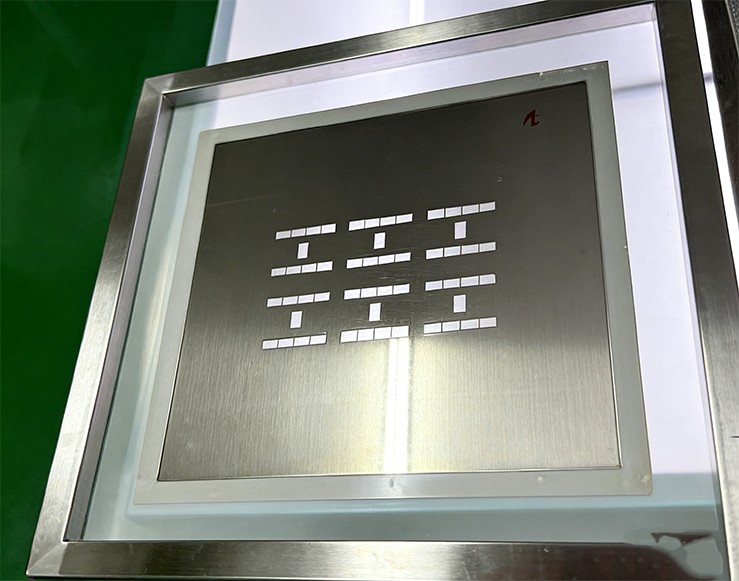
Electroforming ABF Substrate Ball Placement Masks leverage precision metal electroforming technology to deliver specialized processing tailored for the ball placement stage of ABF (Advanced Packaging Substrates). The core product—ABF substrate ball placement masks—serves as a critical supporting component in the advanced semiconductor chip packaging sector. This process combines photolithography masks with metal electroplating technology to precisely replicate nanoscale ball placement hole structures. Utilizing high-performance metals such as nickel and nickel-cobalt alloys, it offers core advantages including accurate ball placement positioning, absence of mechanical stress, excellent dimensional consistency, and chemical corrosion resistance. It effectively addresses traditional pain points of ball placement masks, such as hole position deviation, edge burrs, and susceptibility to deformation. The product meets the high-precision ball placement requirements of ABF substrates, providing precise support for chip placement positioning in the packaging process. It is widely applied in advanced packaging for various IC chips, semiconductor sensors, and other products, driving the development of chips toward higher density, miniaturization, and enhanced reliability.

Product Features
1. Nanometer-level ball placement accuracy: Leveraging Precision Electroforming and deep ultraviolet lithography technology, ball placement holes achieve ±0.1μm diameter precision with positioning error ≤±0.05μm. Minimum hole diameter reaches 5μm, ensuring uniform ball size and precise positioning during ABF substrate ball placement to significantly boost placement yield.
2. Perfectly Formed Ball Placement Hole Structure: Supports high-density ball placement hole layouts with smooth, burr-free walls and no flared deformation. Precise, controllable hole spacing enables densities ≥2000 holes/mm², meeting ABF substrate high-density placement demands while preventing issues like misalignment and short circuits.
3. Zero Mechanical Stress and Deformation: Utilizes non-contact metal deposition technology, eliminating mechanical cutting and heat-affected zones. Preserves original material mechanical properties, prevents residual stress and deformation in the stencil, and maintains flatness ≤0.01mm. Ensures perfect alignment between the stencil and ABF substrate during ball placement.
4. Superior Chemical Corrosion Resistance: Constructed from corrosion-resistant materials like nickel-cobalt alloy and 316L stainless steel, it withstands chemical agents such as flux, etching solutions, and cleaning agents during ABF substrate ball placement and packaging processes. Long-term use shows no material peeling or hole wall damage, significantly extending service life.
5. High Consistency in Mass Production: Automated electroforming production lines and AI vision inspection systems provide real-time monitoring of critical parameters like ball placement hole diameter, position, and surface roughness. Mass-produced masks achieve ≥99.8% consistency and a high yield rate of 99.7%, meeting the demands of semiconductor packaging mass production.
6. Flexible Customization for Diverse Packaging Needs: Supports customization of ABF substrates in various specifications. Ball placement hole size, density, and layout can be adjusted according to customer requirements, accommodating mainstream packaging processes like BGA, QFP, and CSP. Capable of handling both small-batch prototyping and large-scale production with 24-hour rapid response.
Product Performance
1. Precision Performance: Ball-implanting hole diameter accuracy ±0.1μm, minimum hole diameter 5μm, hole positioning accuracy ≤±0.05μm, flatness ≤0.01mm, hole wall roughness Ra≤0.05μm, free of burrs and serrations. Ensures precise ball positioning with a ball-implanting yield rate ≥99.5%.
2. Mechanical Properties: Nickel-cobalt alloy material achieves hardness up to HV550+, tensile strength ≥600MPa. Withstands high-temperature and high-pressure conditions during ball placement without deformation or damage. Service life exceeds 800 ball placement cycles, reducing packaging costs.
3. Environmental Adaptability: Withstands over 1000 hours of corrosion testing and resists chemical agents including flux, etching solutions, and cleaning agents. Operates stably within -30°C to 120°C, maintaining consistent performance without degradation in semiconductor packaging facilities' controlled temperature and humidity environments.
4. Ball Placement Compatibility: Accommodates ball placement requirements ranging from 0.1mm to 0.5mm. Ball placement holes achieve ≥99.9% alignment with solder balls, effectively preventing issues like ball misalignment, bridging, and cold solder joints. This enhances chip packaging reliability and electrical performance.
5. Production Performance: Samples delivered within 24 hours; batch orders fulfilled in 7-10 days. Fully automated production lines enable closed-loop control throughout the process. Metal ion recovery rate exceeds 90%, with energy consumption reduced by 35% compared to traditional processing, balancing environmental sustainability and production efficiency.
6. Compatibility Performance: Fully compatible with all ABF substrate specifications and mainstream ball placement equipment. Seamlessly integrates with advanced chip packaging workflows while supporting diverse flux types and ball materials to meet varied packaging requirements.
Product Application Fields
1. IC Chip Manufacturing: Core application in the lithography process for logic chips, memory chips, power chips, and other ICs. Serves as the critical masking component for pattern transfer, precisely replicating chip circuit patterns to advance miniaturization and high-density development. Suitable for chip manufacturing in mobile phones, computers, servers, and other end devices.
2. Semiconductor Sensor Industry: Manufactures MEMS sensors, optoelectronic sensors, pressure sensors, and other semiconductor sensors. Through precise micro/nano pattern masking, it enables sensor miniaturization and high precision, serving smart wearables, automotive electronics, industrial control, and other applications.
3. Micro-Electro-Mechanical Systems (MEMS) Field: Supports manufacturing MEMS gyroscopes, MEMS accelerometers, and microfluidic chips. Leveraging complex pattern formation capabilities, it enables precision processing of MEMS device structures, enhancing sensitivity and stability.
4. Semiconductor Packaging: Processes lead frame and bump masks in chip packaging, precisely controlling pattern dimensions to enhance packaging accuracy and reliability. Supports mainstream packaging technologies including BGA, QFP, and CSP.
5. Optoelectronics: Used in manufacturing optoelectronic devices like optical communication chips, laser chips, and display panel driver chips. High-precision pattern masks enable accurate formation of optical paths and circuits, enhancing optoelectronic performance.
6. Other Semiconductor-Related Fields: Also applicable to processing semiconductor test fixtures, nanoimprint templates, and other products. Provides high-precision, high-reliability mask plate support services for upstream and downstream semiconductor supply chains, driving high-quality development in the semiconductor industry.
Contact:赖先生
Phone:+86 18938693450
Tel:0755-2708-8292
Email:yw9@zldsmt.com
Add:深圳市宝安区福永镇新和村福园一路华发工业园A3栋
 Zhuolida