Welcome: Shenzhen Zhuolida Electronics Co.TD
Language:
 ∷

∷
∷
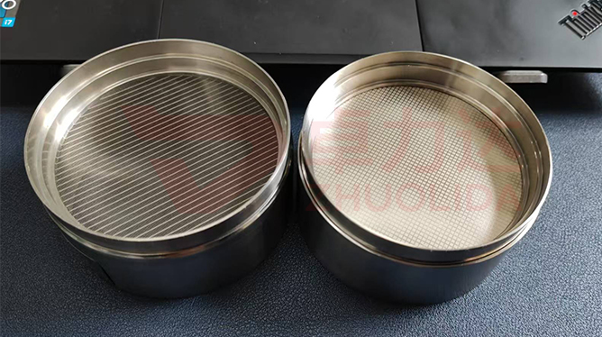
Artwork data only becomes a resist cavity on the substrate after three moves — lamination, laser direct writing and development — and nickel then grows solely on the exposed conductive surface. LDI lamination exposure electroforming governs that transfer. An imported LDI writes the line width into the dry film at 8 μm/8 μm resolution, ±5 μm double-side alignment registers the front and back patterns, and six laser heads sweep a 610×660 mm panel at 90 faces per hour. The finished contour equals the resist contour, so any deviation left by exposure or development is copied 1:1 into metal and no amount of machining afterwards will remove it. Substrates of 0.03–5 mm and four source bands at 365/380/395/405 nm all serve one purpose: straight resist walls and an accurate pattern.
Once deviation enters the resist there is no second chance. Nickel grows along the resist wall, so a wall one degree off produces a wall one degree off in the part; resist left by development covers conductive surface that should be exposed, and no metal grows there; a bubble trapped during lamination scatters exposure energy at that point and leaves a rounded notch after development. Double-sided work is harder still. The ±5 μm figure is the registration error between front and back resist patterns: misregister them and the nickel wall of a through structure picks up a step or an offset layer, more visible the higher the aspect ratio, which is why AOI has to catch it right after development. The 8 μm/8 μm figure answers whether the feature can be made, ±5 μm answers whether front and back line up, and the development window answers whether the resist wall stands. Exposure energy and developer flow already differ between the edge and centre of a 610×660 mm panel, so without zone-by-zone logging the line width of a dozen sheets on one panel will scatter. When a finished contour fails re-measurement, the trail usually leads back to lamination or development, not to the plating bath.
Parameter Window
• Maximum substrate 610×660 mm, minimum 100×100 mm, several sheets per panel
• LED sources 365/380/395/405 nm, chosen by resist thickness and photosensitivity
• Substrate thickness 0.03–5 mm; thin sheets need wrinkle and bubble control during lamination
• Resolution 8 μm/8 μm, setting the smallest writable line width
• Double-side alignment ±5 μm, where front-to-back registration is locked
• Six laser heads at 90 faces per hour
Manufacturing Process (8 Steps)
1. Artwork preparation — output master data to 8 μm/8 μm line width, with allowance for development undercut.
2. Pre-treatment — clean and conductivise 0.03–5 mm substrates, fixing surface cleanliness first.
3. Lamination — bond dry film under controlled temperature and pressure to exclude bubbles, film thickness by aspect ratio.
4. LDI exposure — six laser heads at 365/380/395/405 nm, 610×660 mm panels at 90 faces per hour.
5. Development — develop inside the energy window, where wall verticality and residual resist are fixed.
6. Electroforming — nickel grows along the resist wall and pattern deviation is copied 1:1 into metal.
7. Demolding and inspection — lift the whole sheet, then stencil checker, vision system, flash measurement and AOI confirm the contour.
8. Packing and shipping — supply alignment and line-width records, with bath data retained by the chemical lab.
Core Advantages
1. True contour — the resist is the master; 8 μm/8 μm line width written once, no further machining.
2. Front-to-back register — ±5 μm held, so through structures show no offset layer or step.
3. Large-panel throughput — six laser heads reach 90 faces per hour on 610×660 mm, with several sheets per panel consistent.
4. Closed inspection loop — AOI, vision and flash measurement stop deviation before electroforming.
5. Controlled development — energy logged by zone, wall verticality and residual resist checkable per panel.
6. Stable replication — the mandrel's three-dimensional shape transfers intact, with a smooth surface needing no cutting.
Typical Applications
• Through stencils and masks at ±5 μm double-side alignment, registered at the transfer stage.
• Fine-line electroformed parts at the 8 μm/8 μm class, contours laser cutting cannot reach.
• Several sheets on one 610×660 mm panel, with comparable line-width data across a batch.
• Precision ball-placement stencils, whose aperture contour is fixed in one resist step.
• Wafer-level masks, where high-aspect-ratio resist walls stand on the development window.
• Complex three-dimensional contours, with mandrel shape copied 1:1 into nickel.
Design and Selection Notes
1. Leave margin on the 8 μm/8 μm line width rather than running the design at the resolution limit.
2. Budget the ±5 μm registration first on double-sided parts; a misaligned through wall is harder to fix than a line-width miss.
3. Grade lamination temperature and pressure by 0.03–5 mm substrate, and guard thin sheets against bubbles throughout.
4. Pick 365/380/395/405 nm by resist thickness; do not force short wavelengths through thick film.
5. Log development energy by zone and check the corners of a 610×660 mm panel separately for residual resist.
6. Run AOI and vision measurement right after development, not after the contour has been plated.
7. Match the 90 faces per hour pace of six heads to bath scheduling so resist moulds are not stored too long.
Seen on its own, LDI lamination exposure electroforming governs not whether a pattern can be drawn but whether the drawn pattern grows into nickel unchanged. The 8 μm/8 μm resolution sets the lower bound on line width, ±5 μm double-side alignment sets front-to-back registration, and lamination plus development set the resist wall profile; only with all three do contours on a 610×660 mm panel avoid failing re-measurement after electroforming. What separates capable lines is rarely how steady the bath is, but whether deviation was stopped after development, before the sheet entered the tank. For orders pushed to the limit on line width and registration, fix source wavelength, zoned exposure energy, the development window and alignment compensation into the process card at sampling stage, then run to that card in production — far cheaper than reworking finished parts one by one. That is where LDI lamination exposure electroforming earns its keep: turning invisible deviation in pattern transfer into parameters that can be logged and re-measured. Lamination development electroforming process and LDI double-side alignment accuracy control go by different names, yet on the shop floor they come to the same sentence: make LDI lamination exposure electroforming show measurable contour fidelity on every sheet.
Contact:赖先生
Phone:+86 18938693450
Tel:0755-2708-8292
Email:yw9@zldsmt.com
Add:深圳市宝安区福永镇新和村福园一路华发工业园A3栋
 Zhuolida