Welcome: Shenzhen Zhuolida Electronics Co.TD
Language:
 ∷

∷
∷
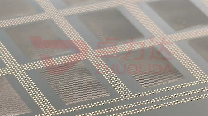
Probe locating template double-side alignment accuracy is the offset between the patterns on the two faces of one substrate, held to ±5 μm with imported LDI exposure. It does not measure whether a single face was drawn correctly, but how the front probe-hole array registers to the alignment features on the back. Wafer test probe locating templates go into semiconductor assembly and test, where the probe tip must pass through a template hole to land on a die pad; shift the hole a little and the tip shifts with it. This figure ties together 8 μm/8 μm resolution, the stitching of six laser heads and substrate thickness from 0.03 to 5 mm, and it is the most direct link between a pattern being made and a probe landing where it should.
Lining up two faces is harder than it sounds. Single-side exposure controls one layer; add a flip and a second clamp and you add a whole family of error sources. A substrate leaving the pre-bake for LDI picks up a few microns from moisture uptake and thermal relaxation; a 0.03 mm foil with one wrinkle on its carrier moves every fiducial; a 610×660 mm panel and a 100×100 mm coupon do not grow by the same amount. LDI runs six laser heads at 90 faces per hour, and if the stitches are not referenced to one datum, a step shows up at the seam once the faces are overlapped. Exposure uses four LED wavelengths, 365/380/395/405 nm, and the resist responds differently to each, so the developed edge shifts by a different amount. More hidden still is electroforming: nickel grows laterally along the resist sidewall, the hole mouth closes in, and the front pattern never moved while the real hole centre has drifted. When a line sees 'single face fully in spec, probe misses after assembly', the cause is usually in these stacked terms. ±5 μm is not one exposure setting; it is what remains after growth, clamping, stitching, undercut and lateral growth have all been pushed down.
Parameter Window
• Double-side alignment ±5 μm (imported LDI); overlay judged by X/Y offset plus rotation
• Resolution 8 μm/8 μm; six laser heads in parallel, 90 faces per hour
• Substrates up to 610×660 mm, down to 100×100 mm, thickness 0.03–5 mm
• Exposure sources: LED at 365 / 380 / 395 / 405 nm, chosen against the resist absorption peak
• Position figures: wafer ball-placement stencil total pitch ±7 μm, aperture size accuracy ±0.003 mm
• Environment: 21±1 °C, 50±5% humidity, with substrates conditioned before loading
Manufacturing Process (8 Steps)
1. Data registration — front and back share one set of datum fiducials, with growth compensation reserved in the layout.
2. Substrate pre-treatment — after cleaning and baking, condition at 21±1 °C; 0.03 mm and 5 mm stock get separate clamping.
3. Lamination — match dry-film tension on both faces; mount thin stock on a carrier so wrinkles cannot pull the fiducials off.
4. Front-side LDI — six heads scan from a calibration table, CCD reads the fiducials as built, each panel gets its own translation and rotation correction.
5. Flip and re-registration — locate from the same datum holes rather than the panel edge, so no clamping error accumulates.
6. Development and electroforming — hold undercut and strike current density down so lateral nickel growth does not eat hole position.
7. Overlay inspection — vision system reads two-face fiducial offset, flash measurement sweeps the panel, stencil checker verifies apertures, AOI finds defects.
8. Compensation write-back — feed measured offsets into the next lot's panel data, converging the specification into ±5 μm batch by batch.
Core Advantages
1. One datum for both faces — fiducials set once and never changed at the flip, so second-registration error does not stack.
2. Per-panel measured correction — LDI adjusts to the fiducials the CCD actually sees, taking substrate growth out on the spot.
3. Large panels stay controllable — 610×660 mm and 100×100 mm calibrated separately, six-head stitches corrected zone by zone.
4. Closed inspection loop — vision system, flash measurement, stencil checker and AOI cross-judge overlay instead of clearing a panel on one reading.
5. Hole position preserved — development and electroforming hold undercut and lateral growth down, so ±0.003 mm apertures do not drift.
6. Batch convergence — offset data written back into layout makes alignment steadier with each repeat of a specification.
Typical Applications
• Wafer test probe locating templates, where the probe tip's reference in assembly and test comes from the double-side aligned holes.
• WLP ball-placement stencils, where ±7 μm total pitch cannot accumulate across the panel.
• ABF substrate Ball and Flux stencils, with openings on both faces registering to each other.
• Probe card guide plates, where alignment passes from layer to layer in a multi-plate stack.
• Fine-pitch BGA and Mini LED printing stencils, whose stepped two-face apertures depend on one datum.
• Electroformed screens and encoder discs with back-side features, located on the back fiducials and not allowed to shift against the front.
Design and Selection Notes
1. Do not skimp on fiducials. Put at least four corner marks on each face; two locating pins cannot stop the panel rotating.
2. Put substrate thickness on the drawing. A 0.03 mm foil and a 5 mm plate need different focus depth, clamping and compensation.
3. Pre-compensate large panels. On a full 610×660 mm exposure, scale artwork from historical growth data rather than waiting for a rescue.
4. Never use the panel edge as datum. Cut-edge tolerance is far larger than ±5 μm; take coordinates from datum holes after the flip.
5. Match film to source. The four wavelengths respond differently, so a film change means re-calibrating pattern-edge shift.
6. Leave room for lateral growth. On ±0.003 mm aperture orders, fix strike current density and resist sidewall angle together.
7. Accept the overlay, not just one face. Two-face fiducial offset plus whole-panel rotation is the error the probe actually sees.
Probe locating template double-side alignment accuracy looks like one number on an exposure tool, yet on an assembly-and-test line it is the boundary between a probe landing on its pad and missing it. ±5 μm carries a lot: growth after conditioning, whether the datum changed at the flip, six-head stitch seams, development undercut, electroform lateral growth. Let any one slip by a micron and it all adds up at the probe tip. When a single face passes re-measurement but the assembled tool misses, the fault is rarely on that face — nobody measured the registration between the two. What makes probe locating template double-side alignment accuracy worth doing is joining CCD readings, vision overlay data and the next lot's compensation into one loop, so the offset converges batch by batch instead of each lot scraping through by sorting panels. Pad pitch keeps shrinking, so the error budget at this layer only gets thinner; get alignment wrong and no probe, probe card or tester downstream can win it back. Fix fiducial layout, datum hole positions, conditioning time and overlay acceptance at sampling stage, then run to that card. Orders that call for probe locating template double-side alignment accuracy should be treated as a system reading: tune it as an exposure setting and you press down only half the error; manage it as a delivery figure and ±5 μm holds.
Contact:赖先生
Phone:+86 18938693450
Tel:0755-2708-8292
Email:yw9@zldsmt.com
Add:深圳市宝安区福永镇新和村福园一路华发工业园A3栋
 Zhuolida