Welcome: Shenzhen Zhuolida Electronics Co.TD
Language:
 ∷

∷
∷
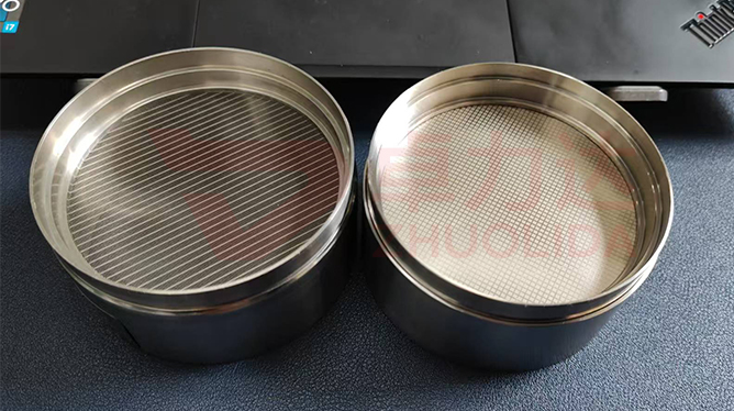
A 4–12 inch WLP ball-placement stencil is pressed onto the wafer. Several hundred thousand to several million 30 μm-class apertures are flooded with solder paste or flux; the squeegee passes, the stencil lifts, and each ball has to stay whole on its pad with nothing clinging to the wall. The wafer ball placement stencil tapered aperture governs exactly that lift. The wall is not a straight bore: the opening side and the contact side differ by a few micrometres of taper, giving the paste a slope along the release direction. A low-adhesion nickel surface then pushes wall surface energy down until adhesion to the paste falls below the paste's own cohesion, so the material lets go of the metal as the stencil rises. Only when wall roughness is held to ≤0.01 μm and aperture accuracy to ±3 μm do taper angle and surface energy become real features of the part rather than lines on a drawing.
The difficulty is that solder paste is not water but a thixotropic body, and flux is stickier still. In a straight-walled hole nearly all release resistance comes from the ring of contact: shrink the aperture to 30 μm on a 15–200 μm stencil and the depth-to-width ratio climbs, so wall contact claims a large share of the paste volume. At the instant of lift, wall adhesion and paste cohesion compete. Raise surface energy slightly and the wall holds the material back, leaving a chipped deposit, insufficient solder or an open joint; reverse the taper so the opening is narrower than the contact side and lifting wedges paste back into the hole, leaving heavier residue. Take pitch from 150 μm down to 100 μm and position accuracy tightens from ±13 μm to ±6 μm, with only tens of micrometres of web left, so a little hanging paste bridges to the neighbour. Extra brightener makes the nickel brighter and drives hardness toward 450–550 Hv, but it also changes the surface state; raising current density from 1 to 4 A/dm² leaves a lot-to-lot difference in wall profile between edge and centre. None of this shows before printing — it appears in the insufficient-solder rate of the first trial sheet, when rework is already too late.
Parameter Window
• Aperture size accuracy ±0.003 mm, total pitch ±7 μm, verified by vision measurement after release
• Minimum aperture 30 μm, thinnest foil 15 μm, smallest opening 40 μm, smallest ball 55 μm
• Aperture wall roughness ≤0.01 μm; the low-adhesion nickel surface is set here
• Pitch of 150/130/110/100 μm maps to position accuracy of ±13/±10/±7/±6 μm
• Nickel alloy hardness 450–550 Hv, thickness tolerance ±3 μm; hardness weighed with surface energy
• Tension 10–55 N with ±1 N internal control; stencil thickness 15–200 μm
Manufacturing Process (8 Steps)
1. Artwork preparation — derive opening data from ball size, add draft compensation for the tapered wall, from hundreds of thousands to millions of apertures.
2. Pre-treatment — clean and conductivise the substrate, passivate the mandrel face for low adhesion, fixing the surface-energy baseline of the nickel.
3. Lamination and LDI — 8 μm/8 μm resolution, ±5 μm double-side alignment, exposure energy graded to the taper to form the angled resist cavity.
4. Development and electroforming — staged current density and brightener control grows nickel along the resist wall into a taper while the low-adhesion surface forms.
5. Demolding — lift the whole sheet from a low-stress corner without dragging the tapered wall or its smooth finish.
6. Stress relief — low-temperature anneal stabilises dimensions so framing does not spring the taper out of tolerance.
7. Inspection — automatic stencil checker reads openings and position, vision system measures taper angle, tension meter confirms 10–55 N.
8. Framing and packing — set tension to band, bond the aluminium frame with AB adhesive, ship with trial-print release records.
Core Advantages
1. Whole-ball transfer — taper gives draft and the low-adhesion face holds adhesion down, so balls stay on the pad instead of the wall.
2. Low insufficient-solder rate — 30 μm-class openings shed their paste cleanly, and bridging risk falls with contact area.
3. Fine pitch usable — the 100 μm pitch band holds ±6 μm position accuracy, with hole position and release behaviour controlled together.
4. Flux compatible — low surface energy sheds flux as readily as paste, so Ball and Flux stencils can be tuned separately.
5. Stable service life — walls at ≤0.01 μm roughness resist residue build-up, reaching 15,000 prints on chip-substrate work.
6. Batch consistency — several sheets from one 610×660 mm panel share one bath, with taper angle and surface energy logged to the same settings.
Typical Applications
• 4–12 inch WLP ball placement, where millions of apertures rule out laser machining.
• ABF substrate ball placement, with Ball and Flux stencils tensioned in separate bands.
• BGA and Mini LED fine-pitch printing, most sensitive to hanging paste at 110 μm and 100 μm pitch.
• Limit stencils of 15 μm thickness and 40 μm openings, where taper makes up for weak release force.
• Micro-ball placement down to a 55 μm ball, with aperture-to-ball diameter at its lower bound.
• Chip-substrate stencils rated for 15,000 prints, where wall condition sets the decay rate.
Design and Selection Notes
1. Fix the taper direction first. The opening side should be slightly larger than the contact side; reversed, it wedges paste into the hole.
2. Write surface energy into acceptance. A low-adhesion nickel surface is not a description but a trial-print insufficient-solder figure.
3. Grade thickness across 15–200 μm; below 30 μm pair the foil with small balls rather than forcing a large diameter.
4. Choose pitch and position accuracy as a pair — 100 μm maps to ±6 μm — instead of watching only the ±3 μm aperture figure.
5. Check wall roughness ≤0.01 μm together with taper angle; lose the finish and adhesion returns.
6. Keep one 10–55 N band per lot and hold the ±1 N control line for consistent release.
7. Where posts or local thickening exist, pick a release direction that avoids the step root of the thickened zone.
Seen on its own, the wafer ball placement stencil tapered aperture governs not whether a hole can be opened but whether the paste agrees to leave it clean. Taper supplies the geometric draft, the low-adhesion nickel surface supplies low interfacial adhesion, and only with both in place do ±3 μm aperture accuracy and the ±6 μm position accuracy at 100 μm pitch survive the first trial print without being erased by insufficient-solder defects. What separates capable lines is rarely how precisely exposure aligns, but whether a dozen sheets from one bath finish with the same set of trial-print data. For orders pushed to the limit on ball diameter and pitch, fix the taper angle, the surface-energy acceptance method, the tension band and the release direction into the process card at sampling stage, then run to that card in production — far cheaper than reprinting sheets afterwards. That is where the wafer ball placement stencil tapered aperture earns its keep: turning the single lift of the stencil into a measurable, repeatable parameter. Low-adhesion nickel surface electroforming and ball-placement stencil paste release process go by different names, yet on the shop floor they come to the same sentence: make the wafer ball placement stencil tapered aperture show a measurable release result on every sheet.
Contact:赖先生
Phone:+86 18938693450
Tel:0755-2708-8292
Email:yw9@zldsmt.com
Add:深圳市宝安区福永镇新和村福园一路华发工业园A3栋
 Zhuolida