Welcome: Shenzhen Zhuolida Electronics Co.TD
Language:
 ∷

∷
∷
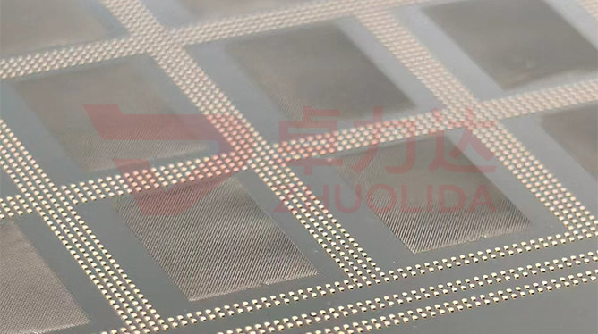
Coat a silicon wafer with photoresist, expose and develop a cavity that is narrow and deep, then grow nickel into it layer by layer and lift it off: the result is a metal mask. Electroformed mask deposition stress control governs that growth. Push the aspect ratio up and electrolyte exchange at the cavity floor slows, so metal-ion concentration spreads out along the depth; any drift in current density, brightener or bath temperature makes deposition rate and internal stress uneven with it. Stress comes in two signs — tensile pulls the mask inward, widening openings or lifting edges off the substrate, compressive pushes thin walls into bulges — while thickness spread makes openings on one part of the sheet larger than another. LDI resolution of 8 μm/8 μm only sets the resist opening; dimensional fidelity of the finished part depends on holding stress and uniformity down together in the bath.
Stress accumulates, and high-aspect-ratio geometry amplifies it. The deeper the cavity, the more transfer relies on diffusion: nickel ions at the floor are not replenished, deposition there runs slower than at the mouth, and grain state and internal stress differ along the wall height. Add brightener and the grain refines, hardness climbs toward 450–550 Hv and internal stress rises with it. Raise current density from 1 to 4 A/dm² and current lines crowd at the edges of a 610×660 mm panel, so corners grow faster and carry higher stress. Let bath temperature wander two or three degrees and stress is no longer uniform across one sheet. None of this shows during deposition — the nickel is constrained by both the silicon substrate and the resist. Release it and the constraint disappears: tensile stress draws the mask inward and a tens-of-micrometres opening can drift by several micrometres, compressive stress wrinkles thin walls, and severe cases lift straight off the substrate. When a post-release re-measure fails on opening size, LDI alignment is rarely the culprit; the deposition stage simply did not hold stress and thickness spread. MEMS evaporation masks, optical elements and semiconductor production masks are accepted in micrometres, so lose this stage and even perfect exposure upstream counts for nothing.
Parameter Window
• LDI resolution 8 μm/8 μm, double-side alignment ±5 μm; the resist opening is fixed here
• Substrate thickness 0.03–5 mm; thin substrates are more sensitive to stress warpage
• Exposure sources 365/380/395/405 nm, four bands chosen by resist thickness
• High-aspect-ratio resist cavities: the larger the ratio, the more transfer is limited
• Nickel alloy hardness 450–550 Hv; hardness and internal stress move together
• Dimensional accuracy taken from vision measurement after release, structural integrity checked per sheet
Manufacturing Process (8 Steps)
1. Substrate preparation — clean and conductivise the silicon, choose 0.03–5 mm by device stiffness.
2. Resist coating — set resist thickness to the target aspect ratio, control coating uniformity first.
3. Lamination and LDI — 8 μm/8 μm resolution, 365/380/395/405 nm exposure, ±5 μm double-side alignment.
4. Development — form the high-aspect-ratio cavity; resist wall verticality sets the nickel wall.
5. Electroforming — zoned current density, temperature and brightener improve deep-cavity transfer and hold stress down.
6. Release — after a low-temperature stress-relief anneal, lift from a low-stress edge without bulging thin walls.
7. Inspection — vision system measures openings and wall angle, hardness tester logs 450–550 Hv, flatness re-checked.
8. Dicing and packing — cut to the device layout, ship with stress and dimension records.
Core Advantages
1. Openings hold size — stress and thickness spread controlled together, so released openings match the design.
2. Thin walls stay flat — compressive stress kept low, fine ribs neither wrinkle nor lift off the substrate.
3. True dimensional fidelity — high-aspect-ratio features stay true along the wall, evaporation patterns stay centred.
4. Batch consistency — several sheets from one 610×660 mm panel share a bath, edge-to-centre rate spread inside the control line.
5. Stable replication — the mandrel's three-dimensional shape transfers in one step, with a smooth surface needing no machining.
6. Traceable — current, temperature, hardness and post-release dimensions logged per sheet, anomalies tracing back to the bath run.
Typical Applications
• MEMS device evaporation masks, where high-aspect-ratio openings are most sensitive to stress release.
• Optical element pattern transfer, where thin-wall flatness sets the clear aperture.
• Semiconductor production masks accepted in micrometres on opening size.
• Wafer-level micro/nanofabrication, electroforming metal masks straight from a silicon resist mould.
• Through structures needing ±5 μm double-side alignment, held in register by controlled stress.
• 0.03 mm thin-substrate masks, supported throughout release to prevent warpage.
Design and Selection Notes
1. Grade the aspect ratio first. The deeper the cavity, the lower the strike current density, so the floor is not starved of ions.
2. Do not over-dose brightener. 450–550 Hv is sufficient; pushing higher drags internal stress up.
3. Set current density by zone and drop the edge zones of a 610×660 mm panel by one band.
4. Hold bath temperature to about ±1 °C; a two- or three-degree drift scatters stress across the sheet.
5. Choose 0.03–5 mm substrate by assembly stiffness; support thin ones throughout release.
6. The 8 μm/8 μm and ±5 μm figures belong to exposure; post-release opening re-measurement is the delivery figure.
7. Log tensile and compressive stress separately and set anneal temperature by stress type rather than one fixed value.
Seen on its own, electroformed mask deposition stress control governs not whether nickel can fill the resist cavity but whether the dimensions still match the artwork once it has. LDI at 8 μm/8 μm with ±5 μm sets the resist; current density, brightener and temperature in the bath set the stress and thickness distribution in the metal. Let the latter slip and the constraint vanishes at release, so tens-of-micrometre openings drift, thin walls bulge, and even perfect exposure upstream cannot be recovered. What separates capable lines is rarely whether a high-aspect-ratio structure can be plated at all, but whether a dozen sheets from one bath finish with the same set of re-measured data. For orders accepted in micrometres on opening size, fix zoned current, brightener concentration, bath temperature and anneal temperature into the process card at sampling stage, then run to that card in production — far cheaper than reshaping sheets after release. That is where electroformed mask deposition stress control earns its keep: turning invisible internal stress into a set of parameters that can be logged and tuned. Wafer mask deposition uniformity and high-aspect-ratio electroformed mask forming go by different names, yet on the shop floor they come to the same sentence: make electroformed mask deposition stress control show measurable dimensional fidelity on every sheet.
Contact:赖先生
Phone:+86 18938693450
Tel:0755-2708-8292
Email:yw9@zldsmt.com
Add:深圳市宝安区福永镇新和村福园一路华发工业园A3栋
 Zhuolida