Welcome: Shenzhen Zhuolida Electronics Co.TD
Language:
 ∷

∷
∷
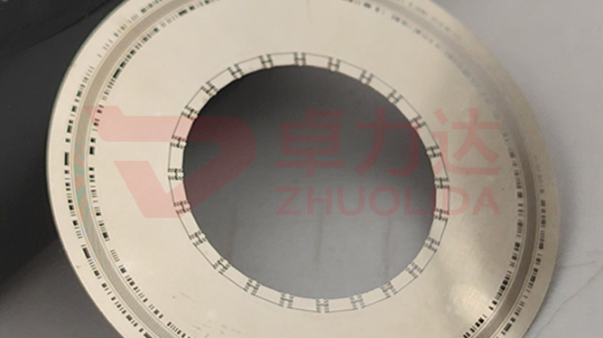
A probe alignment template bolted into a test fixture can pass ±7 μm position and ±3 μm aperture checks and still refuse to take a probe, and the cause is usually the invisible slope at the hole mouth. Probe alignment template guide hole forming is not just about piercing the hole; it also cuts a lead-in angle at the mouth so a tip offset by a few microns is still guided in, and holds wall roughness to ≤ 0.01 μm so nodules on the nickel do not catch the probe. None of it appears on a ±3 μm aperture report, yet it decides whether a probe slides in or butts against the rim: with no lead-in angle a tip strikes and bends, and with a rough wall a few hundred insertions shed debris and jam the hole. It comes down to two things: a slope at the mouth and a clean wall behind it.
On the floor this is usually blamed on incoming probes first. A batch goes on the machine, probes strike off-centre and leave a bright scratch; strip it down and ±7 μm position still holds, but side-lighting shows the mouth is a straight right angle with no lead-in slope at all, so the tip skids sideways on contact. Switch bath lots and the same template grows a burr at the rim before two thousand insertions; section it and the wall is dotted with fine nodules that scrape plating off the probe and pack the debris into the hole. More subtle still: push current density too low chasing a clean wall and the developed resist sidewall leans outward slightly, copying into the nickel as a reverse taper — the probe goes in but hangs on the step coming back out. None of these faults fall inside the opening judgement of an automatic stencil checker, and by the time they surface the whole batch is usually mounted in fixtures. Probe alignment template guide hole forming is harder to land than dimensional inspection precisely because the lead-in angle is a slope and the wall is a side face, both out of reach of a flat-bed checker.
Parameter Window
• Guide hole aperture accuracy ±3 μm and position accuracy ±7 μm, lead-in angle and wall re-checked separately
• Wall roughness ≤ 0.01 μm, held to 0.008 μm internally, nodules sampled per bath
• Minimum aperture 30 μm and ball-template total pitch ±7 μm; the lead-in angle must not eat into usable hole depth
• LDI resolution 8 μm/8 μm and double-side alignment ±5 μm, the lead-in taper shaped by stepped exposure
• Current density 1–4 A/dm², the wall section run at the lower end for slow deposition and finer grain
• Nickel alloy hardness 450–550 Hv, wall finish consistent across a maximum substrate of 610×660 mm
Manufacturing Process (8 Steps)
1. Artwork preparation — master data for the probe array, with the mouth lead-in angle drawn as its own layer.
2. Pre-treatment — substrate cleaning and conductive coating, low-adhesion passivation of the mandrel to avoid strike nodules.
3. Lamination and LDI — imported stepped LDI exposure at 8 μm/8 μm resolution and ±5 μm double-side alignment; resist sidewall and lead-in taper set together.
4. Development — control concentration and time so no residue stays at the foot and the sidewall is not undercut; the lead-in slope is fixed here.
5. Electroforming — staged control of current density at 1–4 A/dm² and bath temperature, nickel copying a clean wall off the resist.
6. Demolding — one-piece release from a low-stress corner; the mouth lead-in angle is most easily pulled flat at lift-off.
7. Inspection — checker for openings, vision and flash measurement for position, profiler sampling wall Ra and lead-in angle.
8. Low-temperature anneal and packing — stress relieved, sorted by 450–550 Hv hardness band, shipped with RoHS records per lot.
Core Advantages
1. Smooth entry — build the lead-in angle properly in probe alignment template guide hole forming and a tip offset a few microns is still guided in.
2. No probe scraping — wall Ra ≤ 0.01 μm keeps nodules from stripping plating off the probe.
3. Truer insertion life — no rim burr, so decay is slower as insertions approach the ten-thousand mark.
4. Dimensions and surface tracked apart — ±3 μm belongs to the checker, lead-in angle and wall to the profiler, so a fault is pinned to a bath run.
5. Large-panel consistency — current banded across 610×660 mm so corner walls are no rougher than the centre.
6. Traceable — stepped exposure dose, current density and sampled Ra go on the process card and reach back to the solution lot.
Typical Applications
1. Wafer probe card guide plates, where dense arrays are most sensitive to the lead-in angle.
2. Alignment holes of 4–12 inch WLP ball-placement templates, where total pitch ±7 μm must hold.
3. Probe guides in ABF substrate test fixtures, where insertion frequency is high.
4. Precision apertures with 20 μm diaphragm ribs, where wall debris blocks the light path.
5. Encoder templates with a 50 μm ±0.5 μm code track, where a shifted hole makes the reading jump.
6. Composite templates with post height or local thickening, whose stepped mouths collapse most easily.
Design and Selection Notes
1. Set the lead-in angle from probe diameter first; in probe alignment template guide hole forming match the mouth slope to the tip chamfer, do not watch only the ±3 μm aperture.
2. Under-dose current rather than over-dose it; at 550 Hv wall striations and internal stress arrive together.
3. Do not rush development; a few tenths of a micron of undercut becomes a step that catches the probe on the nickel.
4. Verify stepped exposure dose per lot; holes short on lead-in taper tend to appear in whole exposure zones.
5. Give wall roughness and lead-in angle their own station, since a flat-bed checker cannot read sidewall Ra.
6. Verify mandrel passivation per lot; nodules start where the conductive layer is uneven.
7. Where local thickening exists, choose a release direction that avoids the step root and keeps the lead-in angle intact.
Seen on its own, probe alignment template guide hole forming barely occupies a standalone step: the stepped exposure dose sets the taper at LDI, development shapes the resist sidewall, the bath decides how nickel grows along that wall, and the few seconds of release decide whether the mouth is pulled flat. Pre-treatment, exposure, deposition and stripping each own a stretch of it, and let any one slip and neither the ≤ 0.01 μm wall nor the lead-in angle will hold. What is hard on a line is not turning out one plate that takes probes smoothly now and then, but keeping a dozen plates from one bath and several consecutive lots inside the same band of taper depth, wall Ra and ±7 μm position — only then does ±3 μm aperture accuracy mean anything. For orders with high insertion counts, fix the stepped exposure dose, the current density curve and development time into the process card at sampling stage and run to that card in production; it is far cheaper than endlessly retuning probe down-force and swapping needles on the tester. On paper probe alignment template guide hole forming is a string of parameters; on the line it is the simple fact that every probe is guided steadily in by its hole mouth.
Contact:赖先生
Phone:+86 18938693450
Tel:0755-2708-8292
Email:yw9@zldsmt.com
Add:深圳市宝安区福永镇新和村福园一路华发工业园A3栋
 Zhuolida