Welcome: Shenzhen Zhuolida Electronics Co.TD
Language:
 ∷

∷
∷
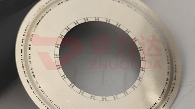
A probe alignment template can hold ±7 μm position after half a year of service and still have its apertures worn a few microns larger, which is rarely a sizing error and almost always a coating hardness that was chosen wrong. Probe alignment template wear-resistant coating process governs the state of the deposited nickel-cobalt layer: keep hardness inside 450–550 Hv with a fine but not brittle grain, and the hole mouth survives repeated probe scraping; below that band the wall grooves quickly and the aperture opens up; above it internal stress climbs and the rim chips at the first knock. None of it appears on the outgoing ±3 μm aperture report, yet it decides whether the template is still usable after insertion counts on the 15,000-cycle scale. It comes down to three things: alloy composition sets hardness, current density sets grain, and a low-temperature anneal lets the stress go.
On the floor this is usually logged as probe wear. A batch runs under three thousand insertions and re-measures 4 μm larger than at shipping; strip it down and the mouth is polished bright, hardness reads only 410 Hv, the nickel-cobalt ratio has drifted and the grain is coarse. Double the brightener in the next bath and hardness jumps to 580 Hv; the mouth no longer collapses, but fine cracks run along the current lines and a corner chips off days later. More subtle still: push current density to the ceiling to clear a backlog and the layer looks dense, yet with no low-temperature anneal the stress stays in, and once mounted in a warm fixture the whole ±7 μm position field drifts a few microns — a flash measurement catches it only after the fact. None of these faults fall inside the opening judgement of an automatic stencil checker, and by the time they surface a whole furnace of boards has usually been scrapped on the tester. Probe alignment template wear-resistant coating process is harder to land than dimensional inspection precisely because hardness and stress are states of the coating itself, which a checker cannot measure.
Parameter Window
• Nickel-cobalt coating hardness 450–550 Hv, held to 480–520 Hv internally, hardness taken per bath
• Aperture accuracy ±3 μm and position accuracy ±7 μm, re-checked before and after insertion testing
• Wall roughness ≤ 0.01 μm, nodules and striations sampled per bath
• Current density 1–4 A/dm², hardness set by alloy ratio and bath temperature rather than heavy brightener dosing
• Low-temperature anneal relieves stress, with position drift held inside ±7 μm across the anneal
• Insertion life verified on the 15,000-cycle scale, aperture growth used as the reject line
Manufacturing Process (8 Steps)
1. Artwork preparation — master data for the probe array, with high-cycle zones flagged for coating requirements.
2. Pre-treatment — substrate cleaning and conductive coating, low-adhesion passivation of the mandrel to avoid strike nodules.
3. Lamination and LDI — imported LDI exposure at 8 μm/8 μm resolution and ±5 μm double-side alignment; the wall profile is set here.
4. Development — control concentration and time so no residue stays at the foot and the mouth is not undercut.
5. Electroforming — nickel-cobalt co-deposition with staged current density at 1–4 A/dm² and bath temperature, locking hardness into 450–550 Hv.
6. Demolding — one-piece release from a low-stress corner; the mouth is most easily pulled into micro-cracks at lift-off.
7. Inspection and anneal — checker for openings, vision and flash measurement for position, then low-temperature anneal, hardness and sampled Ra.
8. Packing — sorted by hardness band, shipped with RoHS records and the insertion verification report per lot.
Core Advantages
1. Apertures resist wear — hold probe alignment template wear-resistant coating process at 450–550 Hv and ±3 μm still holds after 15,000-cycle-scale insertions.
2. No rim chipping — hardness kept below the ceiling and stress relieved by low-temperature anneal, so corners do not crack.
3. No probe scraping — wall Ra ≤ 0.01 μm keeps striations from stripping plating off the probe.
4. Stable lots — nickel-cobalt ratio, current density and anneal curve go on the process card, so hardness reaches back to a bath run.
5. Fewer changeovers — life verified by cycle count rather than feel, so fixture downtime between plate swaps stretches out.
6. Traceable dimensions — ±7 μm position measured before and after insertion, drift logged on its own.
Typical Applications
1. Wafer probe card guide plates, with the highest insertion counts and the hardest demand on coating hardness.
2. Alignment holes of 4–12 inch WLP ball-placement templates, where total pitch ±7 μm must hold over time.
3. Probe guides in ABF substrate test fixtures, where continuous furnace runs leave no room for a mid-run swap.
4. Encoder templates with a 50 μm ±0.5 μm code track, where mouth wear pulls the reading off.
5. Precision apertures with 20 μm diaphragm ribs, where coating debris blocks the light path.
6. Composite templates with post height or local thickening, where stress concentrates at stepped mouths.
Design and Selection Notes
1. In probe alignment template wear-resistant coating process fix the hardness band before the chemistry; 450–550 Hv is the line between wear resistance and brittle cracking.
2. Under-dose the brightener; push hardness past 550 Hv and striations and internal stress arrive together.
3. Stage current density across 1–4 A/dm² rather than running the ceiling for throughput; coarse grain catches up later.
4. Never skip the low-temperature anneal; measure ±7 μm position on both sides of it before release.
5. Take hardness per bath and sample Ra per bath, since a flat-bed checker cannot judge coating state.
6. Re-verify nickel-cobalt ratio with each solution lot; let the ratio drift and hardness falls with it.
7. Where local thickening exists, choose a release direction that avoids the step root and keeps micro-cracks out of the mouth.
Seen on its own, probe alignment template wear-resistant coating process barely occupies a standalone step: the nickel-cobalt ratio is fixed when the bath is made up, grain grows as current density and temperature dictate, a low-temperature anneal lets the stress go, and the few seconds of release decide whether the mouth picks up a micro-crack. Pre-treatment, exposure, deposition and annealing each own a stretch of it, and let any one slip and the 450–550 Hv band will not hold. What is hard on a line is not turning out one hard-enough plate now and then, but keeping a dozen plates from one bath and several consecutive lots inside the same band of hardness, wall Ra and post-anneal ±7 μm position — only then does ±3 μm aperture accuracy mean anything. For orders with high insertion counts, fix the nickel-cobalt ratio, the current density curve and anneal temperature into the process card at sampling stage and run to that card in production; it is far cheaper than swapping plates early and recalibrating probes on the tester. On paper probe alignment template wear-resistant coating process is a string of parameters; on the line it is the simple fact that a plate reaches end of life with its apertures still unopened.
Contact:赖先生
Phone:+86 18938693450
Tel:0755-2708-8292
Email:yw9@zldsmt.com
Add:深圳市宝安区福永镇新和村福园一路华发工业园A3栋
 Zhuolida