Welcome: Shenzhen Zhuolida Electronics Co.TD
Language:
 ∷
∷

∷
∷
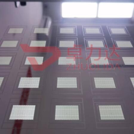
ABF electroforming templates are high-precision molds manufactured via advanced electrochemical deposition and photolithography molding processes, made of high-purity nickel and nickel-cobalt alloy for core ball mounting procedures of chips packaged on ABF substrates. Free of mechanical cutting stress and high-temperature thermal damage, the product delivers micron-level high-precision hole forming and pattern replication, thoroughly resolving defects including burrs, deformation and hole position deviation seen on conventional templates. Integrated molding of microholes and special-shaped holes is supported with superior dimensional consistency and pattern fidelity, requiring no secondary processing. Compatible with advanced chip processes of 7nm and below, the templates serve as core matching components for high-precision chip ball mounting and solder paste printing, widely applied in high-end semiconductor packaging. With smooth hole walls and optimized demolding performance, they effectively reduce tin beads and insufficient solder to boost production yield, meeting mass production demands for high-density, fine-pitch advanced packaging chips in communication, computing and automotive electronics sectors.
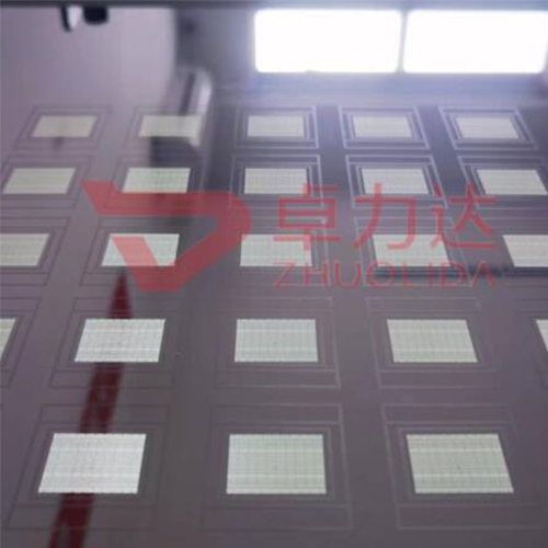
Damage-free advanced process: Integrated electroforming deposition eliminates mechanical cutting and laser thermal damage without internal plate stress, preventing template warpage, deformation and cracking for long-term precision mass production.
Ultra-high pattern fidelity: Precise positioning by photolithography masks realizes over 99.5% pattern reproduction accuracy, featuring clean, burr-free and collapse-free hole edges without post-polishing.
Strong structural adaptability: Integral forming of microholes below 50μm, special-shaped holes and stepped holes; customizable thickness ranging 20–300μm to satisfy diverse demands of high-end packaging.
Excellent demolding performance: Smooth hole walls with optimized tapered cross-section and low-adhesion surface treatment minimize solder paste residue, tin beads and insufficient solder defects to raise printing yield.
Durable & easy maintenance: High-hardness substrate with great wear and chemical corrosion resistance tolerates repeated cleaning and high-frequency mass production, boasting far longer service life than etched and laser templates.
Dimensional precision: Micron-level tolerance control; overall dimensional tolerance ±0.005mm, hole precision up to ±0.001mm, ball positioning error within ±5μm.
Surface property: Hole wall roughness as low as Ra 0.05μm; flat and smooth board surface ensures uniform solder paste adhesion and smooth demolding without tin adhesion.
Stable performance: Stress-free forming guarantees outstanding batch dimensional consistency; high temperature and acid-alkali resistance prevents deformation and precision degradation during long-term use.
Mass production performance: Compatible with large-scale manufacturing and high yield; matches advanced packaging processes of 7nm/5nm chips for high-pin-count precision ball mounting.
Material performance: High-purity nickel-cobalt alloy substrate with high hardness and toughness resists wear and deformation, extending template service life and cutting production costs.
High-end semiconductor packaging: FC-BGA, BGA and CSP packaging on ABF substrates for precision chip ball mounting and solder paste printing, supporting advanced chip processes of 7nm and below.
Communication chips: Widely used in packaging of 5G/6G RF chips, baseband chips and high-speed communication chips to meet high-pin-count and high-density ball mounting precision requirements.
AI computing chips: Applied to packaging of AI chips, GPUs and computing processors to ensure precision and stability of high-density fine-pitch solder joints.
Consumer electronics chips: Precision ball mounting and packaging for main control and storage chips of mobile phones, tablets and smart terminals.
Industrial control & automotive electronics: Packaging of automotive power chips, industrial precision chips and IoT chips, complying with high-reliability standards for industrial and automotive grades.
Contact:赖先生
Phone:+86 18938693450
Tel:0755-2708-8292
Email:yw9@zldsmt.com
Add:深圳市宝安区福永镇新和村福园一路华发工业园A3栋

 Zhuolida