Welcome: Shenzhen Zhuolida Electronics Co.TD
Language:
 ∷

∷
∷
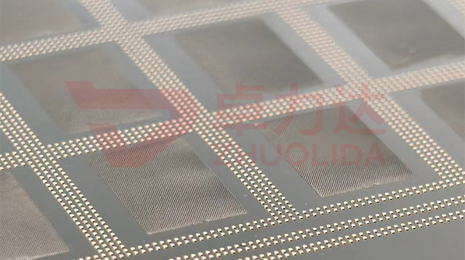
This plate is not a printing stencil. A wafer bumping stencil builds bumps on 8–12 inch wafers, with apertures closing toward 30μm and total pitch held to ±7μm; a printing stencil faces PCB pads and a squeegee and is checked against a different set of rules. Wafer bumping stencil aperture taper control is about walls that are not vertical: the paste-entry opening is slightly wider than the wafer-facing side, forming a 1–3° positive taper, and the taper angle is the difference between the two openings divided by plate thickness. That slope governs whether paste or flux releases as one block and how much volume each aperture transfers; once the volume scatters, reflowed ball diameter and height scatter with it. WLP bump arrays are less forgiving than SMT pads, so taper is a standalone acceptance item here, not something carried on the aperture-size report.
On the floor the taper problem is usually pinned on the paste or the machine. One lot of 12 inch WLP bumping stencils measured inside ±3μm on every aperture, yet post-ball inspection found ball diameter wandering in the edge zone, with bump height in the same row differing by a dozen microns; side lighting showed paste clinging to the walls. Another lot switched to thinner stock, developer undercut ate the entry opening wider, the as-built taper came out steeper than designed, and bridging plus oversized balls showed up after reflow. More subtle still: every sheet from one bath passed on its own, but on the tool the center-to-edge ball diameter distribution would not line up, traced to higher edge current density during electroforming that let the taper drift along the radius. Wafer bumping stencil aperture taper control is hard because the automatic checker scans flat aperture outlines and cannot compute that wall slope; by the time ball diameter scatters, a whole wafer of bumps is already built.
Parameter Window
• Minimum aperture 30μm, total pitch ±7μm; taper computed per aperture from the two opening sizes
• Positive wall taper 1–3°, entry opening wider than wafer-facing side; angle = opening difference / plate thickness
• Aperture accuracy ±3μm and position accuracy ±7μm, judged separately from taper
• Wall roughness ≤0.01μm; a smoother wall releases paste more cleanly and lets the angle relax half a notch
• Plate thickness 15–200μm in classes; every step up changes electroforming growth time
• Nickel-cobalt alloy hardness 450–550Hv, current density 1–4A/dm²; hardness and rate lock the taper together
Manufacturing Process (8 Steps)
1. Data and drawing — set the two opening sizes aperture by aperture from the bump map; the smaller the taper, the tighter the developer undercut allowance.
2. Pretreatment — clean and conductivize the base, passivate the mandrel face so plating starts evenly without nodules.
3. Lamination and LDI — 8μm/8μm resolution, double-side alignment ±5μm; any offset between the two openings is fixed here.
4. Developing — control developer concentration and time, back out the entry-side undercut from the taper, leave no residue at the bottom.
5. Electroforming — current density 1–4A/dm² in staged control with edge current compensation, stop the moment target thickness is reached.
6. Demolding — peel the electroformed part off the mandrel from a low-stress corner so apertures do not collapse and the taper holds.
7. Low-temperature anneal — relieve internal stress in the nickel-cobalt alloy so the plate stays flat and full-field taper does not drift with position.
8. Inspection and framing — an imager and a flash gauge verify both openings, then mount to the ball-placer fixture and log the bath run.
Core Advantages
1. Ball diameter pulls in — holding wafer bumping stencil aperture taper control in one class narrows reflowed height and diameter together.
2. Clean release — a 1–3° positive taper paired with ≤0.01μm walls drops paste as one block with no tails.
3. No need to lean on thin stock — pick a thickness class by taper instead of thinning everything to force release.
4. Anomalies trace to a step — ±3μm aperture accuracy goes to the checker, taper to developing and electroforming, down to a bath run.
5. Full-field consistency — with edge current compensation the center and edge of the wafer no longer separate.
6. Traceable — every sheet logs measured openings, thickness, taper and anneal lot, traceable to a bath run.
Typical Applications
1. 8–12 inch WLP wafer-level bumping stencils, where a million apertures must transfer the same paste volume.
2. Flux printing plates for CSP and BGA bumping, where fine holes let developing pull the taper off target.
3. Fine-pitch Flip-Chip wafer bumping stencils, where taper drives ball diameter at pitch ≥120μm.
4. Micro-bump plates for interposers and silicon bridges, where total pitch ±7μm and taper are checked together.
5. Stepped bumping plates with local thickening, where taper is checked on each side of the step.
6. FOPLP panel-level bumping plates, where whole-sheet taper uniformity holds ball diameter consistent.
Design and Selection Notes
1. Separate the product lines first. Wafer bumping stencil aperture taper control governs bump paste volume, not the area ratio and squeegee settings of a printing stencil.
2. Compute taper from measured openings, not aperture size alone — ±3μm can pass while taper scatters and ball diameter still scatters.
3. Leave a separate allowance for developer undercut. A few tenths of a micron at the entry opening steepens the taper, so recheck against the as-built value.
4. Thickness and taper move together. Step thickness up a class and electroforming time and edge current compensation move with it.
5. Read wall roughness alongside it — Ra≤0.01μm widens the usable taper window by a notch.
6. Double-side alignment ±5μm is the premise; once LDI offsets the two openings, a positive taper turns into a reverse one.
7. Sample the full field, not just the center. Take first and last holes and the four corners radially, measure both openings with an imager or flash gauge, then compute taper.
Break wafer bumping stencil aperture taper control apart and it owns no single step: LDI and developing fix the difference between the two openings, current density and growth time in the bath decide which way the walls lean and by how much, and the few seconds of demolding plus the anneal each guard one stretch. If any of them loosens, the 1–3° positive taper will not hold. Taper drifts with thickness lot, develop time and in-bath current distribution, so it has to be sampled per bath and along the radius. What is hard is not producing one sheet with even balls by chance, but keeping a dozen sheets from the same bath and several consecutive lots sitting in the same taper class at center and edge — only then do ±7μm total pitch and ±3μm aperture accuracy mean anything. For orders with a hard requirement on WLP bumps, fix the target opening sizes, thickness, develop time and current compensation in the process card at sampling and run production to that card; it is far cheaper than endlessly tuning demold speed, swapping paste and wiping the plate at the ball placer. This is the bumping stencil's own ledger; do not apply a printing stencil's acceptance sheet to it.
Contact:赖先生
Phone:+86 18938693450
Tel:0755-2708-8292
Email:yw9@zldsmt.com
Add:深圳市宝安区福永镇新和村福园一路华发工业园A3栋
 Zhuolida
