Welcome: Shenzhen Zhuolida Electronics Co.TD
Language:
 ∷

∷
∷
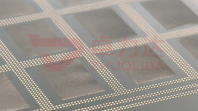
A step stencil carries two thicknesses on one sheet: local thickening under the large pads, a thin web for fine pitch, and between them the ramp from thick to thin is the transition zone. It never appears on the aperture dimension sheet, yet it decides whether the squeegee climbs over smoothly and whether paste piles up at the boundary. The step height grows by a second electroforming deposit, and the ramp width, edge angle and internal stress are all fixed inside this short stretch. Step stencil transition zone forming control governs the geometry and stress of that ramp: the thickening follows the solder volume the pads need, and the edge still has to leave a window for squeegee contact. Too steep and the blade bounces; too gradual and it eats into usable print area.
Step stencils that come back for rework almost always fail at the transition, not in the thickened zone. One lot pairing a QFN large pad with 01005s ran 100μm thick and 40μm thin with a 60μm step and no ramp: the squeegee jumped at the step edge, two rows of fine-pitch pads starved, and wiping did not bring the volume back. SPI pinned the drop within 2mm of the boundary on the thin side. Another lot went the other way, stretching the ramp so long that it swallowed part of the neighbouring 01005 aperture area; a spot meant to stay 40μm was dragged to 70μm and the area ratio collapsed. Subtler still, current crowded into the transition during the second deposit and internal stress lifted the step edge slightly off the board; after a few prints tension fell from 45N to 38N, the checker measured every aperture in spec, and the press still could not lay a solid deposit. None of this shows on a dimension report: the checker scans aperture outlines and nobody logs the stress at the step root or the ramp angle, so by the time it is seen a whole carrier panel is scrap. Step stencil transition zone forming control has to treat the transition as its own process step, not release it mixed into the aperture dimensions.
Parameter Window
• Base thickness 15–200μm in classes: 30–50μm thin web, 80–120μm locally thickened
• Step height 20–60μm set to the real thickening capability of the plant, no universal tolerance written on the drawing
• LDI resolution 8μm/8μm, double-side alignment ±5μm, thickened edge held within ±7μm of the apertures
• Current density 1–4A/dm² in stages, one notch lower in the transition to avoid stress piling at the step root
• Tension 10–55N (±1N internal), checked at three points across the thick-thin boundary
• Nickel alloy hardness 450–550Hv, print life rechecked at 15000 cycles with the step edge still flat
Manufacturing Process (8 Steps)
1. Data and drawing — mark the thickened zone from pad solder demand, set the thin-web class, step height and ramp width.
2. Pretreatment — clean and conductivize the base so the first deposit lays even and the second does not blister at the boundary.
3. Lamination and LDI — 8μm/8μm resolution, double-side alignment ±5μm; the thickened outline and apertures align in one shot.
4. Developing — hold developer concentration and time, leave no residue or undercut at the step edge so the ramp boundary stays clean.
5. First electroforming — grow the 30–50μm thin base at 1–4A/dm² and stop the moment the class is reached.
6. Second thickening — continue plating only in the thickened zone to 80–120μm, drop current in the transition to draw out the step.
7. Release and anneal — peel the whole sheet from a low-stress corner, then low-temperature anneal to relax stress at the step root.
8. Inspection and mounting — checker scans apertures, imager and flash gauge measure the step edge, tension set in 10–55N steps, AB adhesive frame before shipment.
Core Advantages
1. Stable squeegee contact — hold step stencil transition zone forming control and the ramp smooths out, killing blade bounce and boundary starvation together.
2. Two classes managed apart — large pads take the thickened zone, 01005s keep the thin web, no need to compromise the whole sheet.
3. Flat boundary — staged current in the second deposit keeps stress low so the sheet sits tight on the PCB.
4. Accurate position — the thickened edge follows double-side alignment and stays within ±7μm without biting neighbouring apertures.
5. Honest life — with margin in the step, the edge stays flat as prints run toward 15000.
6. Traceable — each sheet records thin-web thickness, step height and ramp width, so anomalies trace back to a bath run.
Typical Applications
1. Printing stencils mixing QFN large pads with 01005 fine pitch, where two thicknesses share one sheet and the step needs the most control.
2. Composite plates with Post or thickened bosses, where the boss-root ramp needs its own squeegee check.
3. 4–12 inch WLP ball-drop templates, where a consistent ball volume is needed across the thickened and thin zones.
4. ABF substrate Ball and Flux plates, thickened side for Ball, thin side for Flux, with no paste crossing the step.
5. Power modules printing large copper areas and fine signal leads on one board, where the step sets single-pass uniformity.
6. Precision sieves for semiconductor material classification, whose framed sheets use the same transition ramp.
Design and Selection Notes
1. Back out thickening from pad solder demand first, then set the thin-web class; do not lift the whole sheet to the thick class.
2. Write step height tolerance from measured plant capability and verify it with a sample before production, not from a drawing of another shop.
3. Read ramp width together with blade hardness and print pressure: too steep bounces, too gradual eats usable area.
4. Continue plating only in the designated zone; a ±5μm double-side alignment drift will bite neighbouring apertures.
5. Measure boundary stress on its own and do not skip the low-temperature anneal; a lifted step is harder to trace than a solder shortage.
6. Set tension in 10–55N steps, check three points at the thick-thin boundary, and never mix classes in one lot.
7. Give step stencil local thickening remeasurement its own station; a checker scanning apertures cannot measure step height or ramp angle.
Break step stencil transition zone forming control apart and no single step owns it: the first electroforming sets the thin-web class, the second deposit draws out the step height, LDI and developing fix the ramp angle, and release plus anneal decide whether the step root lifts. Pretreatment, exposure, two deposits and peeling each guard one stretch, and if any loosens the squeegee jumps at the step edge. The step follows current density and deposit time, so it has to be sampled per bath as a thickness profile instead of judged from final total thickness. What is hard is not one sheet that happens to contact smoothly, but a dozen sheets from the same bath and several consecutive lots all sitting in the same step and ramp class. Only then does ±7μm position accuracy mean anything. For orders mixing pads whose solder volumes differ by several times, fix thin-web thickness, thickening and ramp width in the process card at the sampling stage and run production to that card; it is far cheaper than endlessly tuning squeegee pressure and swapping paste at the printer. Step height tolerance must be set against real plant capability and rechecked on a sample before it goes on the drawing.
Contact:赖先生
Phone:+86 18938693450
Tel:0755-2708-8292
Email:yw9@zldsmt.com
Add:深圳市宝安区福永镇新和村福园一路华发工业园A3栋
 Zhuolida
