Welcome: Shenzhen Zhuolida Electronics Co.TD
Language:
 ∷

∷
∷
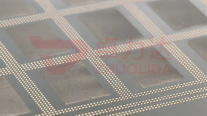
On an electroformed mask, what really decides where the evaporated pattern lands is often not the openings but the few alignment marks at the four corners. They are crosses or dots electroformed together with the pattern, and the mark center relative to the pattern array is the alignment datum the part hands to the client. Electroformed mask alignment mark precision control governs the graphic position accuracy of these marks: shift a mark a little and the whole pattern moves with it, and no fixture on the client side can compensate. Deposition stress and defect inspection are already calibrated; the hard part is imaging marks and openings on the same substrate in one pass so they do not drift apart. How the mask mates to the fixture is a client-side scenario, so this article stays with the datum deviation the part itself can deliver.
Masks that come back from the field almost always measure fine on opening size; the fault sits in the marks. One six-inch evaporation mask held every opening position inside ±7μm, yet the deposited pattern came out a dozen microns off. An imager scan of the marks showed two of the four cross centers shifted 6μm from the drawing: the mark layer and pattern layer had not registered during LDI double-side alignment. The fixture datum never moved; the part datum was skewed on its own. Another lot was worse: developer undercut ate the round marks smaller, roundness dropped, the client alignment camera could not lock the center, and the same sheet landed differently on every remount. One more lot skipped a full low-temperature anneal, internal stress bled out of the thin mask slowly, and a remeasurement found the mark spacing had shrunk a few microns: it passed at the plant and was out of spec at the client. A fully automatic stencil checker misses all of this when it scans openings, because it does not recognise mark graphics; datum deviation needs its own remeasurement on an imager and a flash gauge, and by the time it shows up the whole mask lot needs rework. Electroformed mask alignment mark precision control has to treat the marks as an independent datum, not release them mixed into opening dimensions.
Parameter Window
• Mark center position accuracy ±7μm, with cumulative spacing deviation relative to the pattern array checked alongside
• LDI resolution 8μm/8μm, double-side alignment ±5μm, mark layer and pattern layer registered in one pass
• Mark line width held to 50μm±0.5μm, cross-arm width deviation marked separately
• Round-mark roundness ±0.002mm, opening aperture tolerance ±3μm computed apart
• Current density 1–4A/dm² in stages, nickel-cobalt alloy hardness 450–550Hv
• Maximum substrate 610×660mm; marks and openings taken from the same sheet so the datum does not drift apart
Manufacturing Process (8 Steps)
1. Data and drawing — set corner mark form and center coordinates from the pattern array, state the datum deviation acceptance value.
2. Pretreatment — clean and conductivize the base so plating starts evenly and marks and openings show no pinholes apart.
3. Lamination and LDI — 8μm/8μm resolution, double-side alignment ±5μm, mark layer and pattern layer imaged together.
4. Developing — hold concentration and time, no undercut at mark edges and no narrowing of cross arms, so the center locks cleanly.
5. Electroforming — current density 1–4A/dm² in stages, stop the moment the thickness class is reached.
6. Release and anneal — peel the whole sheet from a low-stress corner, low-temperature anneal to relax stress and hold datum spacing.
7. Inspection — checker scans openings, imager and flash gauge remeasure mark centers and roundness.
8. Datum remeasurement and shipment — issue mark coordinates and datum deviation per sheet, with measured data handed to the client.
Core Advantages
1. Accurate landing — hold electroformed mask alignment mark precision control and the pattern does not shift as a whole, so the fixture datum needs no compensation.
2. True registration — mark layer and pattern layer aligned in one LDI pass, no independent drift within ±5μm double-side alignment.
3. Stable over time — low-temperature anneal relaxes internal stress so datum spacing does not shrink between plant and press.
4. Center locks cleanly — round-mark roundness ±0.002mm keeps the client alignment camera steady across remounts.
5. Traceable — every sheet ships with measured mark coordinates and datum deviation, so anomalies trace back to a bath run.
6. Clear boundary — only part precision is delivered; how it mates to the fixture is set by the client from the measured data.
Typical Applications
1. Fine masks for OLED evaporation, where a slightly shifted corner mark moves the whole panel pattern.
2. Semiconductor wafer evaporation masks, where the mark datum decides whether multi-layer overlay registers.
3. Masks for optical coating, where round marks let an alignment camera lock the center.
4. Wafer-level micro-hole meshes and classification sieves, whose marks and openings are imaged on one sheet.
5. Encoder discs and code-track plates, where 50μm±0.5μm line width also rests on the datum.
6. MEMS and sensor thin-film evaporation masks, where small lots and many variants depend most on per-sheet remeasurement.
Design and Selection Notes
1. Fix the pattern array before mark coordinates, and write the datum deviation acceptance value on the part drawing, not just the opening tolerance.
2. Mating with the evaporation fixture is a client-side scenario; this article covers only the mark position accuracy the part can deliver.
3. Register mark layer and pattern layer in one LDI pass; two exposures throw away the ±5μm double-side alignment.
4. Do not rush developing on round marks; a few tenths of a micron of undercut drags roundness and center repeatability down together.
5. Do not skip the low-temperature anneal; stress left in place passes at the plant and goes out of spec at the client.
6. Sample datum spacing per bath for electroformed mask alignment mark precision control; scanning openings alone cannot show a mark shift.
7. Give mask alignment mark remeasurement its own station; an imager and flash gauge issue a coordinate report, a checker does not recognise mark graphics.
Break electroformed mask alignment mark precision control apart and no single step owns it: drawing fixes the mark form, LDI and developing register the mark layer to the pattern layer, the bath decides which thickness class to stop at, and release plus anneal decide whether datum spacing slowly shrinks. Pretreatment, exposure, deposition and peeling each guard one stretch, and if any loosens the four corner marks will not hold. Datum deviation follows double-side alignment and deposition stress, so it has to be sampled per bath instead of judged from opening scans alone. What is hard is not one sheet that happens to land true, but a dozen sheets from the same bath and several consecutive lots all sitting in the same mark-center class. Only then does ±7μm position accuracy mean anything. For multi-layer overlay orders with many variants, fix the mark form, the alignment class and the anneal conditions in the process card at the sampling stage and run production to that card; it is far cheaper than recalibrating the fixture again and again on the client side. How the mask mates to the fixture follows the client measurement, so recheck the acceptance value against the per-sheet datum remeasurement report before it goes on the drawing.
Contact:赖先生
Phone:+86 18938693450
Tel:0755-2708-8292
Email:yw9@zldsmt.com
Add:深圳市宝安区福永镇新和村福园一路华发工业园A3栋
 Zhuolida
