Welcome: Shenzhen Zhuolida Electronics Co.TD
Language:
 ∷

∷
∷
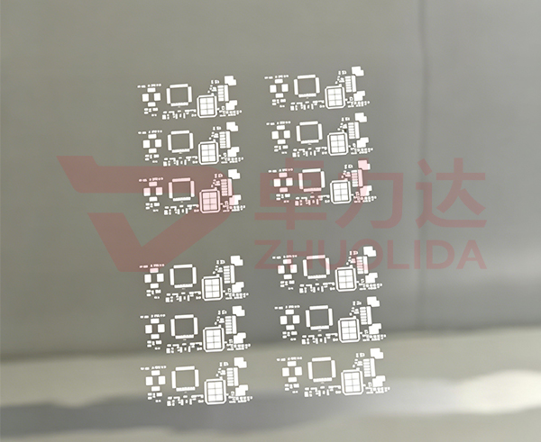
Wafer bumping electroforming template is a precision nickel-cobalt tool used in wafer-level packaging (WLP) to define the solder bump openings for electroplating, flux printing, and under-bump metallization (UBM) processes. Unlike etched stencils that rely on chemical subtraction, electroforming builds the template additively by pulsed electrodeposition on a lithographic master, producing vertical, mirror-smooth micro-apertures with minimal side etch. This geometry keeps solder paste and flux release clean, reduces bridging, and supports the fine pitch required by flip-chip, wafer-level CSP, and 2.5D/3D bumping. Typical materials are low-stress nickel-cobalt alloys, thickness 0.06–0.20 mm, with aperture tolerance in the ±1–2 µm range.
Parameter Window
• Material: Low-stress nickel-cobalt alloy
• Thickness Range: 0.06–0.20 mm
• Aperture Tolerance: ±1–2 µm
• Aperture Wall Roughness: Ra ≤ 0.6 µm
• Tension Stability: 38–45 N/cm
• Minimum Aperture: down to 50–100 µm class
Manufacturing Process / Workflow (8 Steps)
1. LDI Mastermaking — Laser-direct-imaging lithographic master defines bump aperture layout.
2. Master Pre-treatment — Clean and activate the conductive mandrel for uniform deposition.
3. Pulse Electroforming (Core Step) — Deposit low-stress nickel-cobalt by pulsed current to build the template.
4. Stress Annealing — Relieve internal stress to prevent warpage and distortion.
5. Tension Setting — Mount and tension the frame for stable printing.
6. Mirror Polishing — Polish aperture walls for clean paste release.
7. Cleaning & Passivation — Ultrasonic clean and passivate in-class.
8. Micron Inspection — Verify aperture size, position, flatness under microscope.
Core Advantages
1. Vertical Aperture Walls — Near-zero side etch gives clean solder release and reduced bridging.
2. Mirror-Smooth Finish — Low wall roughness improves paste transfer and stencil life.
3. Ultra-Fine Pitch Support — Suited to flip-chip and WLP bump pitches below 200 µm.
4. Low Internal Stress — Annealed nickel-cobalt resists warpage on large reticles.
5. Tension Stability — Consistent frame tension across long print runs.
6. Wear Resistance — Nickel-cobalt withstands high-volume bumping without deformation.
Typical Applications
• Flip-Chip Bumping — Solder bump plating and flux printing.
• Wafer-Level CSP — Fine-pitch ball array deposition.
• 2.5D/3D Packaging — Silicon interposer bumping.
• UBM Process — Under-bump metallization plating mask.
• Cu Pillar Bumping — Copper pillar and cap plating.
• WLP RDL Printing — Redistribution layer paste and flux.
Design Notes & Process Considerations
1. Compensate aperture layout for wafer pad position and print alignment.
2. Balance template thickness against bump volume and paste release.
3. Low-stress anneal is mandatory for large-field, high-density reticles.
4. Mirror polish aperture walls to prevent solder residue and bridging.
5. Validate tension and flatness before production ramp.
6. Match aperture geometry to bumping chemistry and ball size.
Contact:赖先生
Phone:+86 18938693450
Tel:0755-2708-8292
Email:yw9@zldsmt.com
Add:深圳市宝安区福永镇新和村福园一路华发工业园A3栋
 Zhuolida