Welcome: Shenzhen Zhuolida Electronics Co.TD
Language:
 ∷

∷
∷
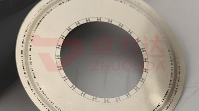
An encoder disc has to carry a 50 μm ± 0.5 μm track, and before any of that the nickel layer must simply stay stuck to the substrate. Encoder disc plating adhesion control governs the invisible interface between the electroformed nickel and the base: what makes a 30–200 μm nickel-cobalt alloy bite into a stainless or glass mandrel, how far activation is pushed in pre-treatment, and whether the atoms laid down in the first seconds of strike are even. Adhesion is not a measure of how hard the coating itself is, but of the grip that refuses to be peeled, judged on the line by the peeled area after a cross-hatch, pull or bend test. It never appears in the track dimensions, yet if the interface is wrong, any later step of etching, dicing or shaft mounting can lift the whole nickel sheet and scrap the disc on the spot.
The trap on the line is treating adhesion as a thickness problem. One lot of 80 μm discs passed the cross-hatch test, then after two hundred hours on a motor shaft the track edge lifted in a fine line; the cause was aged activation solution and an uneven conductive layer, with the nickel peeling slowly along that weak ring. On a rushed lot, low-temperature annealing raised a field of fine blisters across the face, and sectioning showed unremoved resist trapped at the interface, so the bond let go the moment heat was applied. More hidden still, a glass substrate sputtered at too low a power gave a pull value that only just passed, yet dicing chipped nickel off along the track. None of these failures appear in a 50 μm ± 0.5 μm track re-check, and by the time they surface a dozen sheets from one bath are usually scrap. Encoder disc plating adhesion control is hard to put into practice precisely because a flat-bed checker cannot read interface quality, so it needs its own station sampling by bath.
Parameter Window
• Nickel thickness: 30–200 μm; thin layers suffer more from interface stress concentration
• Track width: 50 μm ± 0.5 μm; a failing interface lifts at the edge first
• Nickel-cobalt hardness: 450–550 Hv; raising hardness means watching internal stress too
• Bath current density: 1–4 A/dm², with the strike run at the lower end for a slow lay-down
• Interface bond: pull-test internal limits banded by substrate, with a separate tie layer for glass mandrels
• Low-temperature anneal: temperature and time fixed in the process card, peel area re-checked after anneal
Manufacturing Process (8 Steps)
1. Substrate pre-treatment — degrease, micro-etch and activate as three separate controls; strike only once the conductive layer is even.
2. Sputtered tie layer — power set by glass or stainless mandrel material, giving the nickel something to bite into.
3. Lamination and LDI — imported LDI exposure at 8 μm/8 μm resolution; the track pattern is shaped here.
4. Development — control concentration and time so no residue stays at the foot; most interface inclusions start here.
5. Electroforming — staged control of current density at 1–4 A/dm² and bath temperature, the first layer laid slowly to hold stress down.
6. Demold and anneal — one-piece release then a low-temperature anneal, relieving stress while peel is re-checked.
7. Inspection — vision and flash measurement re-check the track, with pull and cross-hatch testing for the interface alone.
8. Dicing and mounting — cut outside the track ring, then check once more for lifted nickel before the disc goes on the shaft.
Core Advantages
1. Stable interface — encoder disc plating adhesion control fixes activation and strike, so peel rejects drop off sharply.
2. Anneal tolerance — no blisters or bubbling after low-temperature anneal, because inclusions are stopped back at development.
3. No nickel loss at dicing — a tie layer matched to the substrate cuts track-edge chipping.
4. One logic across gauges — 30–200 μm layers share the same pre-treatment approach, so changing thickness does not mean re-tuning the bath.
5. Traceable — activation concentration, strike current and pull value are logged per bath, so a fault reaches back to a lot.
6. Reliable on the shaft — at high speed the nickel does not creep up along a weak interface, so the track stays put over time.
Typical Applications
1. Incremental optical encoder discs, where fine tracks are most sensitive to edge lift.
2. Absolute multi-track discs, where many layers accumulate stress and demand more of the bond.
3. Servo motor feedback discs, whose interface must survive repeated shear at high start-stop rates.
4. Reflective glass-substrate discs, which need a tie layer before nickel will grip at all.
5. Large-diameter metal discs, where 30–200 μm nickel concentrates more internal stress.
6. High-stability discs that must be annealed, where interface quality decides whether blisters appear.
Design and Selection Notes
1. Set pre-treatment by substrate first. Stainless takes micro-etch activation; glass always needs a sputtered tie layer.
2. Run the strike slow rather than fast. Laying the first layer at 1–2 A/dm², even atoms matter more than building thickness.
3. Log activation concentration per bath; aged solution gives an uneven conductive layer and the bond collapses at that ring first.
4. Do not rush development. Resist trapped at the interface turns into blisters the moment anneal heat is applied.
5. Read hardness and internal stress together. At 550 Hv the risk of interface peel rises instead of falling.
6. Give encoder disc plating adhesion control its own station; pull and cross-hatch testing cannot be folded into dimensional inspection.
7. Fix the anneal curve in the process card and run to it in production; that is far cheaper than rework after mounting.
Seen on its own, encoder disc plating adhesion control barely fills a standalone step: the interface is set by substrate pre-treatment and the sputtered tie layer, the first seconds of strike decide whether atoms go down evenly, and resist residue, the anneal curve and dicing stress each own a stretch of it. Let any one slip and a 30–200 μm nickel layer can lift as a whole sheet. Interface bond follows the activation lot and bath temperature, so it has to be sampled per bath rather than let one pull value speak for a whole run. What is hard on a line is not turning out one firmly stuck disc now and then, but keeping a dozen sheets from one bath and several consecutive lots free of weak interface at the track edge, only then does 50 μm ± 0.5 μm track accuracy mean anything. For orders that run at high speed and must pass a low-temperature anneal, fix activation concentration, the strike current curve, sputter power and anneal time into the process card at sampling stage; running to that card beats rework after mounting and endlessly picking over discs at inspection. On paper encoder disc plating adhesion control is a few groups of numbers; on the line it is the plain fact that every disc survives dicing, annealing and high-speed rotation without shedding nickel.
Contact:赖先生
Phone:+86 18938693450
Tel:0755-2708-8292
Email:yw9@zldsmt.com
Add:深圳市宝安区福永镇新和村福园一路华发工业园A3栋
 Zhuolida
