Welcome: Shenzhen Zhuolida Electronics Co.TD
Language:
 ∷

∷
∷
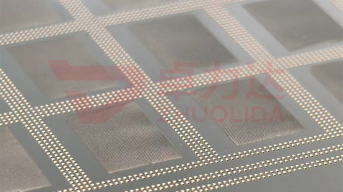
Tens of thousands of pads sit on one silicon substrate, and getting every mask aperture onto its pad does not depend on the apertures themselves but on a few unassuming crosses and code tracks at the four corners. Electroformed mask alignment mark forming governs how that datum set grows on the same foil as the nickel apertures: LDI writes the mark pattern into the resist, nickel grows along the resist sidewall in the same bath, and marks and apertures share one deposition and one release, so their relative position never passes through a second alignment step. On the tool a vision system reads the mask marks, compares them with the substrate fiducials, and solves the shift and rotation before clamping. A mark is usually a cross frame plus a 50 ± 0.5 μm code track, with grating ribs held to 20 μm — legible without stealing active area. It takes no part in deposition, yet it decides whether ±7 μm aperture position accuracy is real.
The costly mistake on the line is treating alignment marks as decoration on the drawing. A batch of WLP deposition masks goes on the tool and the vision system keeps failing to acquire the marks; strip one down and the cross edges have been blurred into rounded corners by a thin nickel skin — lateral growth ate the 20 μm rib width and the recognition threshold collapsed on the spot. Switch bath lots and the marks read fine and overlay looks correct, yet the third wafer drifts as a whole; re-measuring shows internal stress was never relieved, framing quietly pulled the marks a few microns away from the apertures, and the ±5 μm double-side budget was gone. More subtle still: developer residue left at the foot of a code track makes the software drop one 50 μm pitch, it solves the rotation angle with the wrong sign, and edge apertures drift out beyond ±7 μm in a systematic way. None of these failures appear in an aperture-size re-check, and by the time the vision system alarms or a film lands off-pad a whole wafer lot is already coated. Electroformed mask alignment mark forming is managed as its own subject precisely because a mark is the measurement datum — once the datum drifts, every dimension downstream drifts with it.
Parameter Window
• Double-side alignment ±5 μm and LDI resolution 8 μm/8 μm; marks and apertures share one exposure datum
• Code track 50 ± 0.5 μm, grating rib 20 μm; cross frame size set by the reading software
• Aperture position accuracy ±7 μm, re-checked against the coordinate frame solved from the marks
• Maximum substrate 610×660 mm; wider corner-mark spacing is harder on nickel flatness
• Nickel-cobalt alloy hardness 450–550 Hv; when hardness rises, watch internal stress and mark corner rounding together
• Overlay error logged per lot; masks beyond ±5 μm never reach the deposition step
Manufacturing Process (8 Steps)
1. Datum design — place four corner crosses and code tracks to the substrate pad map, write the mark frame into the master data.
2. Pre-treatment — clean and conductivise the substrate, passivate the mandrel face so strike nodules cannot bury the mark feet.
3. Lamination and LDI — double-side overlay exposure writes marks and apertures into the resist in one pass at 8 μm/8 μm, alignment held to ±5 μm.
4. Development — control concentration and time so no residue stays at the code-track foot and the 20 μm rib is not thinned by undercut.
5. Electroforming — stage current density at 1–4 A/dm² to suppress lateral growth before the 50 μm track can blur.
6. Demold and anneal — one-piece release from a low-stress corner, then low-temperature anneal to relieve stress and lock mark-to-aperture spacing.
7. Inspection — vision system solves the mark frame, flash measurement sweeps apertures, an automatic stencil checker re-checks ±7 μm position.
8. Framing and packing — AB adhesive bonds the aluminium frame, tension set in a 10–55 N band, mark coordinates re-read before shipping.
Core Advantages
1. One datum — electroformed mask alignment mark forming puts marks and apertures in a single deposition, removing a second overlay step.
2. Fast setup — the vision system reads all four corners at once and solves shift and rotation directly, with no manual hunting.
3. Traceable budget — ±5 μm overlay and ±7 μm position are booked separately, so a fault points to exposure or framing.
4. Thin ribs hold — corner rounding on a 20 μm grating rib stays controlled, so the threshold does not collapse between bath lots.
5. Large-format ready — a 610×660 mm span is wide, and low-temperature anneal flattens the nickel waviness that comes with it.
6. Traceable — mark re-measurement values and overlay error are stored per sheet, traceable back to a specific LDI run.
Typical Applications
1. WLP wafer-level deposition masks for 4–12 inch wafers, where apertures must register to substrate pads one by one.
2. Mini LED and BGA fine-pitch printing stencils, found on the tool by their corner marks.
3. Ball and Flux stencils for ABF substrates, whose double-side alignment leans on one shared datum set.
4. Precision grading screens for semiconductor materials, delivered with their assembly datum on the foil.
5. Micro-aperture screens with grating ribs, where a 20 μm line is fussiest about mark clarity.
6. Large photovoltaic grids, where four corner marks over a 610×660 mm field set whole-sheet alignment.
Design and Selection Notes
1. Align the mark frame to the substrate fiducial drawing first, do not back-solve it after electroforming.
2. Cut code tracks to 50 ± 0.5 μm and confirm the pitch the reading software expects up front.
3. Estimate lateral growth from foil thickness; the compensation for a thin foil is not the same band as a 200 μm sheet.
4. Do not rush development — a trace of residue at a code-track foot is enough to make the software drop one pitch.
5. Relieve internal stress by low-temperature anneal and read mark coordinates both before and after framing.
6. Set tension within one 10–55 N band and never mix bands in a lot, or mark-to-aperture spacing will not match.
7. Scrap a master whose double-side overlay exceeds ±5 μm rather than gambling on it at the deposition stage.
Seen in isolation, electroformed mask alignment mark forming barely owns a standalone step: the frame is fixed in the master data, the mark profile takes shape in LDI and development, nickel stress settles during deposition and anneal, and the moment of framing can gently pull the whole datum off. Let any one stretch slip and the shift and rotation the vision system reads no longer mean anything. What is hard on a line is not producing one mask that registers, but holding the corner marks and apertures of a dozen sheets from one bath, across several consecutive lots, inside the same band — only then does ±7 μm position accuracy mean anything. For orders with a hard overlay requirement, freeze datum placement, code-track pitch, double-side error and the anneal curve into the process card at sampling, and run to that card in production; it is far cheaper than endlessly retuning clamp pressure and hunting for alignment on the vision system after mounting. On paper electroformed mask alignment mark forming is a few crosses and a string of parameters; on the line it is the fact that every sheet can carry its apertures to directly above the substrate pads on one shared datum.
Contact:赖先生
Phone:+86 18938693450
Tel:0755-2708-8292
Email:yw9@zldsmt.com
Add:深圳市宝安区福永镇新和村福园一路华发工业园A3栋
 Zhuolida
