Welcome: Shenzhen Zhuolida Electronics Co.TD
Language:
 ∷

∷
∷
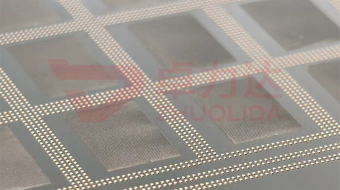
A wafer bumping stencil that has run a few thousand prints is rarely scrap across the whole plate; more often a few apertures are worn, a wall is scored, or an edge is pitted by flux. Wafer bumping stencil rework and reuse governs which plates can be saved, how they are built back up, and on what evidence they return to the line: scan the full field first, mark worn, clogged and scored zones, and scrap anything with a broken rib, wide distortion or tension out of band. For the rest, mask everything but the openings to be repaired, add nickel by local re-electroforming to a target thickness, then develop or micro-machine the size back. Passing is not looking flat; the repaired zone is compared point by point with the original data — ±3 μm apertures, ±7 μm position and wall Ra ≤ 0.01 μm all back in band — tension returned to a 10–55 N band, and remaining life estimated from prints still available, with margin left as 15,000 cycles approach.
The common trap is treating rework as adding nickel and grinding it flat. A batch runs true for two wafers, then the repaired apertures lay down too much; measurement finds them a few microns large because re-electroforming current ran high, overbuilding thickness that was never machined back. Switch lots and the repair layer differs in hardness from the base, delaminating at the repair edge on release — the checker scanning the flat face misses it, and burrs show at the rim only at assembly. Worse is stress: local deposition drags neighbouring apertures by a few microns, so the repaired hole passes while its neighbour pushes past ±7 μm. None of these show in a single-hole dimensional recheck, which is why wafer bumping stencil rework and reuse compares the whole field to the original data rather than passing one repaired hole.
Parameter Window
• Reworkable criteria: local wear, ribs intact, tension still inside a 10–55 N band
• Dimensional recovery: ±3 μm apertures and ±7 μm position after repair, checked against original data
• Wall roughness ≤ 0.01 μm, no nodules or step marks left in the repaired zone
• Local re-electroforming current density 1–4 A/dm² at the low end for slow build, no overthickness
• Nickel alloy hardness 450–550 Hv, repair-to-base hardness gap controlled against delamination
• Reuse life: estimated from remaining prints, margin left as 15,000 cycles approach
Manufacturing Process (8 Steps)
1. Incoming assessment — full-field checker scan, worn, clogged and scored zones marked, rework or scrap decided.
2. Cleaning and stress relief — separate-bath flux removal, low-temperature annealing to steady the datum.
3. Local masking — resist over sound areas, only the openings to be repaired exposed.
4. Local re-electroforming — slow deposition at the low end of 1–4 A/dm² to target thickness with machining allowance.
5. Development and micro-machining — repaired openings returned to 30 μm class, deburred without touching neighbours.
6. Demasking and cleaning — resist stripped, plating solution cleared, no bath crystals left.
7. Inspection — checker for ±3 μm apertures and ±7 μm position, vision comparison with original, profiler sampling Ra.
8. Re-framing and packing — tension back to a 10–55 N band, clean sealed, remaining life labelled.
Core Advantages
1. Less scrap — make wafer bumping stencil rework and reuse work and local damage need not retire a whole plate.
2. Dimensions recovered — repaired zones compared to original data, ±3 μm and ±7 μm both back in band.
3. No delamination — repair hardness matched to base, no peeling on release, no rim burrs.
4. Neighbours stay put — masking plus annealing keeps repair stress from dragging adjacent apertures.
5. Life is quantified — reuse judged by remaining cycles, not by how flat the plate looks.
6. Traceable — incoming scan, repair bath run and recheck data filed per plate.
Typical Applications
1. WLP wafer bumping templates for 4–12 inch wafers, high unit cost makes local wear worth repairing.
2. Ball and Flux stencils for ABF substrates, where flux-pitted local gaps can be rebuilt.
3. Mini LED and BGA fine-pitch printing stencils, where a collapsed aperture can be recovered locally.
4. Micro-hole screens for semiconductor material grading, clogged zones reopened after repair.
5. Composite stencils with post height or local thickening, where step wear can be patched in place.
6. Large-format photovoltaic grid stencils, where edge damage need not replace the whole sheet.
Design and Selection Notes
1. Decide reworkability first. Broken ribs, wide distortion or tension out of band go to scrap, not repair.
2. Expose only the openings to be repaired; keep the masking edge off neighbouring apertures.
3. Hold repair current at the low end, 1–2 A/dm² slow build with machining allowance left.
4. Anneal before repair, or neighbouring apertures get dragged past ±7 μm afterwards.
5. Recheck the whole field against original data, not only the one repaired hole.
6. Keep the hardness gap inside 450–550 Hv so repair and base do not sit in different bands.
7. Log remaining life on the lot card and leave margin before approving reuse near 15,000 cycles.
Seen on its own, wafer bumping stencil rework and reuse is not one repair step but a chain of decisions: the incoming scan draws the reworkable line, masking fixes which apertures get built up, repair current decides whether thickness overshoots, micro-machining brings size back to the original, and a full-field recheck decides whether the plate returns to the line. Cleaning, annealing, masking, deposition and recheck each own a stretch, and let any one slip and ±3 μm apertures and ±7 μm position will not come back into band, neighbours drifting with the stress. What is hard on a line is not one plate repaired well now and then, but a batch of reworked plates and several reuse rounds sitting in the same repaired-zone hardness, dimensional and remaining-life band — only then is it safe to schedule them into production. For cost-sensitive orders with tight registration, fix the reworkable criteria, repair current curve and full-field comparison items into the rework card at sampling stage and release to that card; it is cheaper than judging flatness by eye or stopping mid-print to swap a stencil. On paper wafer bumping stencil rework and reuse is a string of criteria; on the line it is every repaired plate continuing to place balls accurately at its original dimensions.
Contact:赖先生
Phone:+86 18938693450
Tel:0755-2708-8292
Email:yw9@zldsmt.com
Add:深圳市宝安区福永镇新和村福园一路华发工业园A3栋
 Zhuolida
