Welcome: Shenzhen Zhuolida Electronics Co.TD
Language:
 ∷

∷
∷
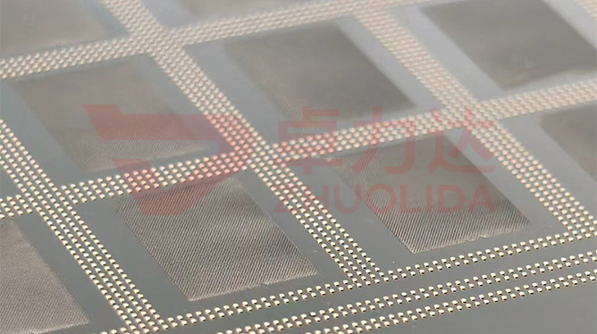
Whether an electroformed mask can go on the line has less to do with how neat it looks than with what hidden flaws the whole sheet carries. Electroformed mask defect inspection process is the gate after demolding and stretching: the nickel foil is bonded to an aluminium frame, then an automatic stencil inspection machine with a vision system and flash measurement sweeps every aperture across the 610×660 mm field, judging pinholes, aperture-to-aperture shorts, broken openings and hole-wall burrs separately before release. It is not the same job as a dimensional spot check: that measures ±3 μm aperture accuracy on a handful of holes, while defect inspection has to cover everything, because one ≥25 μm pinhole that slips through turns into a field of bridged pads at deposition. The hard part is telling a real defect from a normal process mark: ≤0.01 μm hole-wall roughness, slight development undercut and edge waviness after stretching all surface in the same grayscale image. Set the threshold loose and defects are missed; set it tight and the screen fills with false calls.
Line-side failures mostly come from criteria that do not follow the bath lot. One fine-pitch mask passed a routine threshold, then bridged across the board on the printer; pulling the grayscale image back showed a ≥25 μm pinhole waved through as hole-wall texture, the machine's gray gate still set for the previous thick-foil lot. Another lot switched to a harder nickel-cobalt alloy at 450–550 Hv, the hole walls reflected more strongly, and the same gate flagged every normal edge as a burr until the review operator simply released the batch in bulk. Nastier still is the half short: a single nickel thread joins two apertures, the ≥50 μm web still holds, the automatic criterion never reaches the short threshold, and the opening only plugs for good after a few prints. Then there is the habit of scanning the centre and spot-checking the corners, when the edge of a 610×660 mm sheet is exactly where stretching stress is messiest and defects cluster tightest. None of these are a broken machine; they are a criterion that took 'what counts as a defect' too lightly. Electroformed mask defect inspection process is managed on its own because defect morphology moves with the bath, thickness and tension, and no single set of thresholds runs from first lot to last.
Parameter Window
• Minimum aperture ≥25 μm; the pinhole criterion sets its detection floor here, never judge below the resolution
• Web ≥50 μm; aperture-to-aperture shorts are judged by residual nickel bridge width against the web
• Aperture accuracy ±3 μm and position accuracy ±7 μm; defects and dimensional drift booked separately
• Automatic stencil inspection machine at 8 μm/8 μm scan resolution, matched to the 8 μm/8 μm LDI output
• Hole-wall roughness ≤0.01 μm; reflectance differences calibrated in gray bands against 450–550 Hv hardness
• Maximum substrate 610×660 mm; corners and centre get zoned thresholds, 100% whole-sheet coverage
Manufacturing Process (8 Steps)
1. Criterion calibration — take coupons from this bath lot, confirm real pinholes versus normal texture by eye, set the gray gate.
2. Zoned thresholds — split the 610×660 mm field into centre and corner bands, write each threshold into the inspection program.
3. Load and locate — align the frame datum to the machine table, back-calculate the coordinate system from marks to avoid scan drift.
4. Whole-sheet scan — the automatic stencil inspection machine images every aperture at 8 μm/8 μm, no spot-check blind zones.
5. Defect classification — pinholes, shorts, broken openings and burrs logged separately by shape and size.
6. Vision re-measure — suspicious points go to a vision system for ±3 μm aperture accuracy, clearing reflectance false calls.
7. Flash position check — flash measurement sweeps all hole positions, confirming no defect rides along with a ±7 μm position error.
8. Release and trace — pass to ship; criterion version and missed-defect review records archived with the sheet.
Core Advantages
1. Nothing missed — electroformed mask defect inspection process scans 100% coverage, catching corner flaws too.
2. False calls held down — gray bands calibrated to hardness and roughness cut the review load.
3. Traceable criteria — each lot's threshold version is archived, so a problem traces back to a specific bath.
4. Clean classification — pinholes and shorts logged apart, rework or scrap decided at a glance.
5. Decoupled from size — defect criteria do not eat the ±7 μm position budget; size and appearance managed on their own.
6. Fast changeover — a new thickness runs a coupon first instead of a veteran operator tuning gates by eye.
Typical Applications
1. 4–12 inch WLP wafer-level deposition masks, where a million apertures cannot spare one missed pinhole.
2. Mini LED and BGA fine-pitch printing stencils, where an aperture-to-aperture short becomes bridged pads directly.
3. Ball and Flux stencils for ABF substrates, where a ≥50 μm web half short hides best.
4. 610×660 mm photovoltaic large meshes, where edge defect density is high and spot checks always miss.
5. Semiconductor grading micro-aperture screens, where ±3 μm aperture tolerance and the pinhole criterion tug at each other.
6. Micro-structured masks with 20 μm grating ribs, where a broken rib and a burr must be judged apart.
Design and Selection Notes
1. Calibrate the gray gate to thickness and hardness first; 450–550 Hv is not one gate.
2. Keep the pinhole detection floor at the 8 μm/8 μm resolution, never write a criterion below what resolves.
3. Set zoned thresholds for centre and corners; one value for a whole sheet always fails at the edge.
4. Judge shorts by nickel bridge width, do not stare at the ≥50 μm web alone.
5. Re-measure every suspicious point on a vision system, never let reflectance false calls pass in bulk.
6. Book defect criteria and ±7 μm position re-checks apart, do not blend them into one report.
7. Re-run coupons when the bath lot changes, since brightener shifts hole-wall reflectance too.
Seen in isolation, electroformed mask defect inspection process adds no machining step; it all rests on the judgement. What a real defect looks like is calibrated on coupons, thresholds are zoned into the inspection program, suspicious points pass through a vision system and flash measurement in turn, and release is the conclusion stacked from those steps. Loosen the gate anywhere and a ≥25 μm pinhole reaches deposition; tighten it and a screen of false calls drags the manual review to a halt. What is hard on a line is not sweeping one clean sheet, but holding centre-to-corner criteria from a dozen sheets of one bath, across several consecutive lots, inside the same band — only then does fine pitch dare go toward ≥25 μm. For orders with a hard yield requirement, freeze the coupon calibration map, zoned thresholds, bridge criterion and review rule into the process card at sampling and run to that card in production; it is far cheaper than finding bridging on the line and digging back through grayscale images. On paper electroformed mask defect inspection process is a few gray bands and one classification table; on the line it is the fact that every sheet, once stretched onto its frame, has its hidden flaws picked clean before it ships.
Contact:赖先生
Phone:+86 18938693450
Tel:0755-2708-8292
Email:yw9@zldsmt.com
Add:深圳市宝安区福永镇新和村福园一路华发工业园A3栋
 Zhuolida