Welcome: Shenzhen Zhuolida Electronics Co.TD
Language:
 ∷

∷
∷
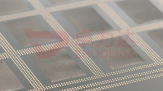
Electroforming is not a one-to-one copy of the master pattern onto nickel. Nickel starts on the conductive layer, grows level with the resist, then keeps spreading laterally along the resist sidewall, so the finished aperture ends up narrower than the one drawn in the master data — all the more so on a thick foil. Electroformed mask pattern compensation process is what folds that extra ring in before the master is cut: estimate lateral growth from stencil thickness, current density and deposition time, pre-enlarge the aperture in the LDI data, and let the nickel close back onto the target size as it grows. The compensation is not one coefficient applied across the whole sheet. A thickness span of 15–200 μm, a current density span of 1–4 A/dm², and development undercut all move that number. Holding finished aperture size to ±3 μm accuracy rests on this pre-correction plus a closed loop that feeds measured results back in.
The usual line-side failure is treating one lot's compensation coefficient as a master key. A 100 μm mask cut with the coefficient from a 30 μm foil comes out of the bath with every aperture a step narrower, micro-holes of ≥25 μm simply plugged, and ±3 μm aperture accuracy out of spec across the board. On another order the schedule pushes current density to 4 A/dm², lateral growth runs harder at the edges where current lines crowd, and one sheet measures true at the centre and undersized at the rim — flash measurement draws it as a gradient band. Then there is the case that leaves development undercut out of the sum: a few tenths of a micron shaved off the resist wall, stacked on deposition growth, over-compensates fine-pitch zones, neighbouring apertures bridge, and the ≥50 μm web floor breaks. Lean too far the other way and the oversized opening dumps extra paste, with BGA bridging climbing again. None of these show up in a master-data check; by the time finished parts are measured a dozen sheets from one bath are already plated. Electroformed mask pattern compensation process is managed on its own precisely because lateral growth follows the bath lot, thickness and current, and no single fixed formula covers it.
Parameter Window
• Stencil thickness 15–200 μm; lateral growth grows markedly with thicker deposits
• Current density 1–4 A/dm²; the high end grows faster laterally and is edgier at the rim
• Minimum aperture ≥25 μm, pitch ≥120 μm, web ≥50 μm
• Aperture accuracy ±3 μm; compensation residual converges to this band
• LDI resolution 8 μm/8 μm and double-side alignment ±5 μm set the smallest usable correction step
• Nickel-cobalt alloy hardness 450–550 Hv; lateral growth rate shifts as hardness is raised
Manufacturing Process (8 Steps)
1. Growth calibration — run coupons at each thickness and current density, measure actual lateral growth.
2. Zoned modelling — split centre and edge into several coefficient bands from the whole-sheet current distribution.
3. Master pre-correction — pre-enlarge apertures in the LDI data by those coefficients and write the values into the process card.
4. Lamination and LDI — output the compensated pattern at 8 μm/8 μm resolution, double-side alignment ±5 μm.
5. Development — control undercut and book the dimensional change it brings into the compensation sum.
6. Electroforming — run 1–4 A/dm² to the calibrated curve and do not change current midway.
7. Demold and anneal — release the whole sheet, low-temperature anneal, measure a sample of finished apertures.
8. Closed-loop re-measure — checker, vision and flash measurement read the residual and feed it back into the coefficient table.
Core Advantages
1. Right first time — electroformed mask pattern compensation process removes lateral growth up front, so finished parts need no rework.
2. Micro-holes stay open — thickness-based compensation keeps ≥25 μm apertures clear after deposition.
3. Whole-sheet uniformity — zoned coefficients flatten the centre-to-edge gradient band.
4. Fine pitch holds — compensation and development undercut booked together bring bridging down.
5. Fast changeover — calibrate a coupon for a new thickness instead of trial and error by a veteran operator.
6. Self-correcting — each lot's residual feeds the coefficient table, so it tightens as it runs.
Typical Applications
1. Mini LED and BGA fine-pitch printing stencils, where small openings are most sensitive to lateral growth.
2. WLP ball-placement templates for 4–12 inch wafers, where a 30 μm minimum aperture must be held exactly.
3. Ball and Flux stencils for ABF substrates, where a ≥50 μm web cannot survive over-compensation.
4. Micro-aperture grading screens for semiconductors, whose ±3 μm tolerance rests on pre-correction.
5. Composite stencils with local thickening, where thick and thin zones need separate growth bands.
6. Micro-structured masks with 20 μm grating ribs, where a small line-width error distorts the pattern.
Design and Selection Notes
1. Calibrate lateral growth by thickness first; 15 μm and 200 μm do not share one curve.
2. Fix current density and leave it — the coefficient is calculated against that current.
3. Measure development undercut on its own, do not fold it into deposition growth as one number.
4. Give centre and edge separate coefficients; one value for a whole sheet always draws a gradient band.
5. Correction steps are limited by 8 μm/8 μm resolution, never write a correction below the resolvable pitch.
6. Sweep finished parts with flash measurement and re-tune the coefficient if residual exceeds ±3 μm.
7. Re-run coupons when the bath lot changes, since brightener shifts the lateral growth rate too.
Seen in isolation, electroformed mask pattern compensation process owns no standalone machine; it all sits on the master data and the deposition curve. Lateral growth is calibrated on coupons, the compensation is written into the LDI data, development adds its own undercut, and the finished size is the sum of those entries. Let any one estimate drift and ±3 μm aperture accuracy will not hold. What is hard on a line is not landing one accurate sheet now and then, but holding centre-to-edge apertures from a dozen sheets of one bath, across several consecutive lots, inside the same band — only then does fine pitch dare go toward ≥25 μm. For orders with a hard dimensional requirement, freeze the thickness-to-current-to-growth table, zoned coefficients, measured undercut and the residual feedback rule into the process card at sampling and run to that card in production; it is far cheaper than reworking compensation values after final inspection. On paper electroformed mask pattern compensation process is a few coefficients and one calibration curve; on the line it is the fact that every aperture stops at target size once deposition ends, with no rescue step needed.
Contact:赖先生
Phone:+86 18938693450
Tel:0755-2708-8292
Email:yw9@zldsmt.com
Add:深圳市宝安区福永镇新和村福园一路华发工业园A3栋
 Zhuolida