Welcome: Shenzhen Zhuolida Electronics Co.TD
Language:
 ∷

∷
∷
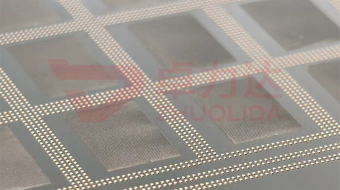
The electroformed mask release process governs how the nickel layer deposited on a silicon substrate is lifted off the wafer face in one piece, without damaging the silicon or distorting the mask. It differs from stencil demolding: a stencil is later stretched onto an aluminium frame, whereas a silicon-substrate mask is the delivered part once lifted, and the wafer usually has to be recovered for reuse. Three relationships at the interface have to be managed together — the conductive seed layer on the silicon surface, the adhesion between that seed layer and the nickel, and the internal stress within the nickel itself. Make the seed layer too friendly and the nickel bites into the silicon, so peel force brings either edge chipping or residual nickel; make it too slippery and the deposit lifts locally halfway through, leaving a gap in the pattern. Damage-free separation means all three settle into place during those few seconds of peeling: the nickel leaves whole, the silicon stays intact, and the ±5 μm double-side pattern does not shift. A stencil can still be pulled back into size by framing afterwards; a silicon-substrate mask has no such buffer, and every debt at the interface is settled the moment it lifts.
Three failures show up most often on the line. One is edge chipping: silicon is brittle, so a lift angle slightly too steep or peel force concentrated at one point breaks a notch out of the rim, and worse, the whole wafer splits along a cleavage plane — the substrate cannot be reused and the mask goes with it. Two is pattern damage: adhesion runs locally high at fine ribs and micro-hole arrays, so hard pulling thins the ribs and leaves residual nickel at the hole rim; a flash gauge finds the opening out of agreement with the design, and the ±5 μm double-side datum drifts with it. Three is release warp: nickel and silicon have very different thermal expansion, and deposition stress sits in the layer pressed flat by the rigid wafer where it cannot be seen. Lift it and the constraint is gone; the thin mask curls at the edge and bows in the middle, and flatness is lost. All three live at the interface, not in exposure or in the bath, and the electroformed mask release process exists precisely to stop force running out of control during those few seconds. That stretch is also the hardest to log: peel force and lift angle ride on technique, so the first pieces in a bath come off clean while later ones chip, and the bath chemistry reads perfectly normal.
Parameter Window
• Silicon substrate up to 610×660 mm, wafer masks managed per piece, substrate reuse count logged.
• Double-side alignment ±5 μm, LDI resolution 8 μm/8 μm; pattern coordinates re-measured after release.
• Mask thickness 15–200 μm; low-temperature anneal temperature and soak time fixed per lot, not adjusted on the fly.
• Current density 1–4 A/dm² in stages, deposition stress pushed low before lifting, never peel with stress still in the layer.
• Nickel alloy hardness 450–550 Hv, wall roughness ≤0.01 μm; hardness weighed together with internal stress.
• Lift starts at a shallow 15–30° angle against the face, peel force capped in bands by wafer thickness so the load never lands on one point.
Manufacturing Process (8 Steps)
1. Wafer pre-treatment — clean the silicon substrate, lay the seed layer by conductive pre-treatment and set adhesion low at the same time.
2. Lamination and LDI — expose after lamination at 8 μm/8 μm resolution and ±5 μm double-side alignment, fixing the pattern datum.
3. Development — develop the resist pattern and confirm fine ribs and micro-hole zones open cleanly before the bath.
4. Electroforming — stage current density at 1–4 A/dm², pressing stress down as the layer grows, thickness held to band.
5. Lift start — raise the nickel from a low-stress corner at a shallow angle, opening a seam along the interface first.
6. Release — lift the whole sheet at controlled angle and speed, backing dense pattern zones before they pass, so force stays spread.
7. Anneal and re-measure — low-temperature anneal relieves stress in the nickel, then vision and flash gauges check pattern and flatness.
8. Substrate reuse — inspect the wafer for chipping and residual nickel; clean acceptable pieces back into the next lot, pack masks separately.
Core Advantages
1. Intact wafer — the electroformed mask release process combines a low-adhesion seed layer with a controlled lift, cutting chipping and cleavage cracks sharply.
2. Undamaged pattern — fine ribs and micro-holes peel with backing, so rib width and hole rims carry no residual nickel and are not thinned.
3. Stable flatness — low-stress deposition plus low-temperature anneal keeps the thin mask from curling or bowing after lift.
4. Coordinates held — ±5 μm double-side readings agree before and after release, so the pattern datum does not move.
5. Reusable substrate — wafers that pass inspection return to the line, spreading the per-piece cost of a wafer mask.
6. Traceable process — lift start point, peel force and anneal temperature logged per piece, anomalies traced back to the bath run.
Typical Applications
1. Silicon-substrate wafer masks, nickel masks for evaporation and sputtering lifted whole from the wafer.
2. Precision screens for semiconductor material grading, thin nickel mesh equally vulnerable to release distortion.
3. Encoder discs and aperture blades with fine ribs, where the outline is most easily torn during release.
4. Large-panel masks with dense pattern zones, several pieces sharing release conditions within 610×660 mm.
5. Sampling and small-lot orders that reuse the wafer, where substrate recovery matters most.
6. Mask parts destined for low-temperature anneal or direct clamping, where release state decides downstream allowance.
Design and Selection Notes
1. Fix the adhesion window first. A seed layer too friendly bites, too slippery lifts; verify thickness per lot.
2. Start the lift at a low-stress corner, never at a dense pattern zone or the step root of a thickened area.
3. Peel at a shallow angle against the face; steepen it and force concentrates, chipping the wafer rim first.
4. Back dense pattern zones with temporary support so fine ribs and micro-holes do not take the peel force alone.
5. Press deposition stress down before lifting, do not hold current density at the 4 A/dm² ceiling for long runs.
6. Put low-temperature anneal after release; reverse the order and the wafer is still there while stress has already pulled the pattern.
7. Inspect every wafer for chipping and residual nickel before reuse; never force a damaged one into the next lot.
Taken apart, the electroformed mask release process is less a final action than an interface audit of pre-treatment, exposure and deposition. A low-adhesion seed layer makes the sheet liftable, low-stress deposition keeps it flat once lifted, and controlled angle and speed keep the wafer unchipped and the pattern intact. Miss any one and the ±5 μm double-side pattern will not hold. What separates capable lines is rarely whether nickel can be grown on silicon at all, but whether a dozen pieces from one bath all lift off in the same state and the wafers still go back intact. For orders that specify wafer mask nickel layer separation, fix seed-layer thickness, lift start point, peel angle ceiling and anneal temperature into the process card at sampling stage, then run to that card in production — far cheaper than paying for every chipped wafer. That is where the electroformed mask release process earns its keep: in a few seconds, splitting a silicon substrate and a nickel layer into two parts that are both still usable. Fixing seed thickness and the angle ceiling costs far less than sorting chipped edges and replacing wafers afterwards.
Contact:赖先生
Phone:+86 18938693450
Tel:0755-2708-8292
Email:yw9@zldsmt.com
Add:深圳市宝安区福永镇新和村福园一路华发工业园A3栋
 Zhuolida
