Welcome: Shenzhen Zhuolida Electronics Co.TD
Language:
 ∷

∷
∷
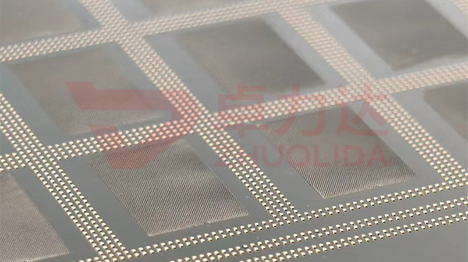
Electroformed mask deposition uniformity control watches whether the nickel layer grows evenly across a whole silicon substrate — concretely, whether the thickness spread from centre to corner can be pulled into a narrow band. It is a different matter from the nominal thickness: hitting 50 μm when 50 μm is called for is not hard, but having every measurement point on a 610×660 mm panel sit close to 50 μm is. Thickness looks like a dimensional figure, yet underneath it is the sum of three things: current density, the distribution of current lines, and bath flow. Current lines crowd naturally at the edge, so nickel grows faster at the rim; in zones with dense openings the real plated area is larger, current is spread thin, and deposition slows again. A little thicker here, a little thinner there, and stress is no longer even after release, so downstream lithography and etching line widths drift. Convergence means flattening all of these deviations together until in-plane thickness spread no longer follows position. A single thickness reading that passes means little; spread the whole panel into a map before you can tell whether the error is corner build-up, banding, or artwork-driven.
Three patterns show up most often in measurement. One is corner build-up: current lines concentrate at the four corners of a large panel, real current density runs above the setpoint, and the nickel there ends up a dozen microns thicker than the centre. Once the spread opens, the corners bear first when the mask is clamped, and flatness is lost outright. Two is banded thin zones: bath circulation is not spread evenly, ion supply lags along certain directions across the face, deposition rate drops, and the thickness map shows thin bands that land right on fine-rib pattern areas, shifting etched line width with them. Three is thickness ripple that follows the artwork: give one current density to the whole panel while sparse and dense opening zones differ several-fold in real plated area, and nickel thickness rises and falls with pattern density — a flash gauge sweeps and reads high and low by turns. None of these come from wrong bath chemistry; they come from current and flow that were never flattened, and that position-dependent error is exactly what electroformed mask deposition uniformity control treats. They also overlap: corners already run thick, and where return flow is poor the local spread climbs well above the centre, which an average thickness figure will never reveal.
Parameter Window
• Current density 1–4 A/dm² supplied by zone, corners stepped down separately, never one value across the whole panel.
• Substrates up to 610×660 mm with 15–200 μm nominal thickness, in-plane spread converged over a grid of at least 3×3 points.
• Mask thickness 15–200 μm, nominal set per product; uniformity and nominal judged separately, not folded together.
• Nickel alloy hardness 450–550 Hv, wall roughness ≤0.01 μm; hardness is not built by local over-plating.
• Double-side alignment ±5 μm, LDI resolution 8 μm/8 μm; pattern density fed into the current zoning basis.
• Bath temperature drift held within ±2 °C, circulation flow tuned to the 610×660 mm format to avoid banded thin zones.
Manufacturing Process (8 Steps)
1. Pattern density analysis — divide the 610×660 mm face into current zones by opening distribution, keeping dense and sparse areas apart.
2. Substrate pre-treatment — clean and render the silicon conductive so seed-layer sheet resistance is uniform and current spreads evenly.
3. Lamination and LDI — expose after lamination at 8 μm/8 μm resolution and ±5 μm double-side alignment to form the resist pattern.
4. Development — develop the pattern, confirm each zone opens cleanly, and log pattern density for the current zoning step.
5. Racking and shielding — add auxiliary cathodes and a shielding frame to draw crowded corner current lines away and flatten them.
6. Zoned electroforming — supply current density 1–4 A/dm² by zone with circulation flow tuned in step, measuring thickness as the layer grows.
7. Whole-panel thickness mapping — vision and flash gauges sweep thickness on a grid, producing an in-plane map rather than a single reading.
8. Feedback loop — fold the thickness spread into the next lot zoning, then release after low-temperature anneal, re-measure and ship.
Core Advantages
1. In-plane consistency — electroformed mask deposition uniformity control holds centre and corners inside one narrow band.
2. Stable flatness — stress distribution follows the uniformity, so the mask does not warp after release or bear on its corners when clamped.
3. Controlled line width — with no thickness ripple, downstream lithography and etching line widths no longer drift with position.
4. Pattern-independent — current zoned by opening density, so nickel thickness in dense and sparse zones does not follow the artwork.
5. Repeatable large panels — several sheets from one 610×660 mm panel share a zoning model, narrowing lot-to-lot thickness spread.
6. Closed-loop traceability — a thickness map is filed per sheet, so anomalies trace back to current zones and flow settings.
Typical Applications
1. Silicon-substrate wafer masks, where whole-panel thickness consistency underpins the evaporation shadow ratio.
2. Precision screens for semiconductor material grading, where mesh thickness uniformity feeds straight into aperture consistency.
3. Encoder discs and aperture blades, where thickness ripple carries into outline and flatness error.
4. Large-format photovoltaic grids, where the 610×660 mm format leans hardest on current zoning.
5. Composite masks with local thickening or posts, where thick and thin zones need separately calculated current.
6. Mask parts destined for etching or a second pattern, where in-plane thickness spread decides line-width allowance.
Design and Selection Notes
1. Draw the current zones first. Cut by opening density, do not feed one value across a whole artwork.
2. Always shield or add auxiliary cathodes at the corners; leave the current lines crowded and those four corners thicken first.
3. Measure seed-layer sheet resistance across the panel; uneven conduction masquerades as uneven deposition, so rule it out first.
4. Tune circulation flow to the format, not just the centre; banded thin zones mostly appear at the edge return flow.
5. Do not let bath temperature wander; beyond ±2 °C local rate pulls apart, and temperature control beats extra brightener.
6. Map thickness on a grid, not a single vision-gauge reading; one point cannot reveal in-plane spread, produce a map.
7. Write thickness spread back into zoning per lot, and re-calibrate whenever the bath or substrate changes.
Traced from the start, electroformed mask deposition uniformity control shows that thickness spread is not caused by deposition alone but is a position function stacked from pattern density, current lines, flow and temperature. Zoned current keeps the corners from taking extra thickness, shielding and auxiliary cathodes flatten the current lines, and whole-panel grid mapping makes the deviation visible. Miss any one and a nominal pass will not buy in-plane consistency. What separates capable lines is rarely whether nickel can be plated to 50 μm, but whether dozens of points on a 610×660 mm panel land in the same narrow band. For orders that specify mask electroforming current distribution, fix the zoning map, shielding scheme, flow settings and grid-thickness criteria into the process card at sampling stage, then run to that card and write back per lot — far cheaper than reworking after release warp or line-width failure. What electroformed mask deposition uniformity control ultimately does is turn something that follows position into a reproducible whole-panel thickness map. Once the zoning map is calibrated, a shift change is just a matter of setting flow to the card, not re-trialling current from scratch.
Contact:赖先生
Phone:+86 18938693450
Tel:0755-2708-8292
Email:yw9@zldsmt.com
Add:深圳市宝安区福永镇新和村福园一路华发工业园A3栋
 Zhuolida
