Welcome: Shenzhen Zhuolida Electronics Co.TD
Language:
 ∷

∷
∷
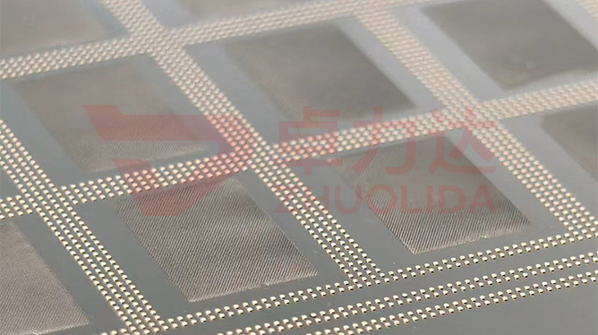
Wafer ball-placement stencil minimum aperture formation governs the hardest openings on a sheet: the nominal 30 μm class, and whether they turn one-to-one from a resist pattern into through-holes in the nickel. It is a different question from position accuracy, which asks whether the coordinate is true; minimum aperture asks whether the hole exists at all, is open, and is large enough. A WLP stencil carries hundreds of thousands of openings, most of them comfortable, but in the fine-pitch zone where pitch is pressed to ≥120 μm the opening shrinks to around 30 μm and the margin for both development and deposition narrows together. Holding aperture accuracy to ±3 μm means a 30 μm hole tolerates only a tenth of that as error: a little resist left behind, one micron too much nickel growth, and it is outside tolerance. That narrowest point of process capability is exactly what 'the boundary' refers to. Treat a 30 μm opening as routine at order review, with no trial coupon for exposure and strike, and this is exactly where production stalls.
Three failures account for most scrap on the floor. One is incomplete development: a 30 μm hole has a large aspect ratio, developer cannot exchange at the bottom, the mouth is already over-developed while a thin film of resist still clings at the base, nickel will not grow there during electroforming, and measurement shows a necked-down opening or a 'blind hole' — a flash gauge sweeps and finds a field of undersized holes. Two is over-development: push time or spray pressure to clear the bottom and the mouth resist undercuts, the wall picks up taper and a rounded corner at the foot, and after release the hole is no longer straight. Three is electroforming closure: at high current density nickel grows faster at the rim than at the centre, sideways growth narrows the 30 μm opening, the mouth seals first while the inside is still hollow, and by the time an automatic stencil checker finds the aperture below tolerance the whole sheet is beyond recovery. All three sit on the capability edge of wafer ball-placement stencil minimum aperture formation, and no increase in sampling ratio will bring them back. They also stack on the same holes: one slightly under-developed is the first to be sealed by sideways growth, so a single step log rarely reveals the root cause.
Parameter Window
• Minimum opening ≥25 μm, production target 30 μm, with pitch ≥120 μm and web ≥50 μm.
• Aperture accuracy ±3 μm, position accuracy ±7 μm; small holes fully inspected by diameter, not folded into sampling.
• LDI resolution 8 μm/8 μm, double-side alignment ±5 μm; exposure dose for the 30 μm zone set as its own window.
• Current density 1–4 A/dm², strike held near 1 A/dm² to suppress sideways closure at the mouth.
• Stencil thickness 15–200 μm; a 30 μm opening suits a thin foil, keeping aspect ratio within reach of the developer.
• Wall roughness ≤0.01 μm, nickel alloy hardness 450–550 Hv; do not chase hardness or stress concentrates at the rim.
Manufacturing Process (8 Steps)
1. Artwork design — flag the 30 μm openings in the fine-pitch zone, set exposure compensation and diameter allowance.
2. Substrate pre-treatment — clean and render conductive so thin resist bonds firmly, reducing blind spots at the hole bottom.
3. Lamination and LDI — expose after lamination at 8 μm/8 μm resolution, giving the 30 μm zone its own exposure dose.
4. Development — control time, temperature and spray pressure so mouth and bottom clear together, then inspect the base for resist under a microscope.
5. Strike plating — start at a low 1 A/dm² so nickel spreads evenly along the wall before current is raised in stages.
6. Deposition and release — zone current density at 1–4 A/dm², then release in one piece and low-temperature anneal for stress relief.
7. Full aperture inspection — an automatic stencil checker and flash gauge measure every 30 μm opening, with a vision gauge confirming the wall.
8. Framing and packing — aluminium frame bonded with AB adhesive, tension graded at 10–55 N so the small-hole zone is not pulled out of shape.
Core Advantages
1. Intact hole shape — wafer ball-placement stencil minimum aperture formation calibrates the 30 μm development window separately, with no resist at the base and no rounded corner at the wall.
2. Diameter held — a low-current strike suppresses sideways growth, so ±3 μm aperture accuracy does not collapse in the fine-pitch zone.
3. Clean release — straight, smooth walls help flux and solder paste transfer, so fewer holes clog during placement.
4. Traceable yield — every small hole is measured and logged, so anomalies trace back to exposure dose and strike current.
5. Thin-foil fit — 15–30 μm foils carry temporary support, so a 30 μm opening does not shrink through release distortion.
6. Batch consistency — several sheets from one 610×660 mm panel share development and strike settings, narrowing lot spread.
Typical Applications
1. 4–12 inch WLP ball placement, where fine-pitch openings are pressed down to the 30 μm class.
2. ABF substrate Ball and Flux stencils, small-opening masks matched to micro-pitch solder balls.
3. BGA and Mini LED printing stencils, where paste release is sensitive to 30 μm hole shape.
4. Precision screens for semiconductor material grading, where micro-hole uniformity sits on the same development edge.
5. Probe positioning templates and other dense arrays, small and tightly packed, most vulnerable to resist residue.
6. Composite stencils with local thickening or posts, where the small-hole zone and the thickened zone need separate current.
Design and Selection Notes
1. Fix the aspect ratio first. Do not pair a 30 μm opening with a thick foil; stay toward the thin end of 15–200 μm so developer reaches the base.
2. Give exposure its own dose. The fine-pitch 30 μm zone should not share one LDI setting with the large-hole zone.
3. Develop in stages rather than one hard pass; over-development at the mouth pulls taper into the wall.
4. Always check the hole bottom after development. Only enter the bath once no resist is visible, do not rely on later inspection to catch it.
5. Keep the strike low, starting near 1 A/dm²; once the mouth closes sideways there is no way back.
6. Do not chase hardness. 450–550 Hv is enough, and stress concentration at the rim deserves more attention than hardness.
7. Grade tension within 10–55 N and keep dense small-hole zones off the upper band, so the holes are not stretched.
Read end to end, wafer ball-placement stencil minimum aperture formation shows that the figure 30 μm is not produced by any single step but by margin given up at two boundaries, development and electroforming. Development delivers a clean base and a straight wall, a low-current strike keeps nickel from swallowing the hole sideways, and per-hole inspection makes the deviation visible on the spot. Miss any one and ±3 μm aperture accuracy will not hold at the finest pitch. What separates capable lines is rarely how tidy the large holes are, but whether the hardest batch among hundreds of thousands all comes out at one diameter. For orders that specify electroformed stencil micro-aperture formation, fix the 30 μm exposure dose, development time, strike current and hole-bottom criterion into the process card at sampling stage, then run to that card in production — far cheaper than reworking sheets after a full inspection fails. What wafer ball-placement stencil minimum aperture formation ultimately manages is nudging that 'one size smaller and it will not open' boundary a little further out. Fixing it in the process card rather than in one operator's hands keeps the fine-pitch yield steady across shifts and bath changes.
Contact:赖先生
Phone:+86 18938693450
Tel:0755-2708-8292
Email:yw9@zldsmt.com
Add:深圳市宝安区福永镇新和村福园一路华发工业园A3栋
 Zhuolida
