Welcome: Shenzhen Zhuolida Electronics Co.TD
Language:
 ∷

∷
∷
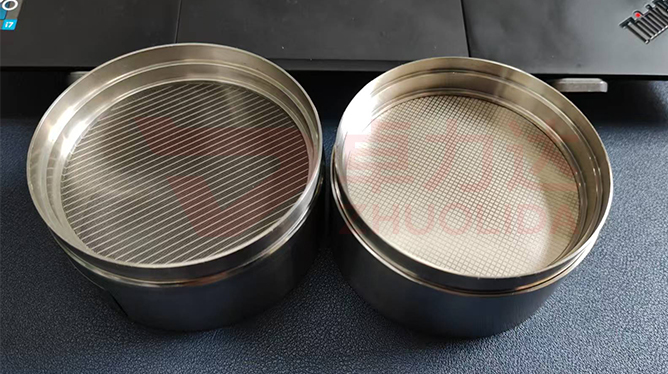
The electroformed screen aperture pattern fidelity control governs how much of the round, square or shaped hole on the drawing survives into the finished nickel mesh: whether roundness has drifted, whether the diameter has grown, whether the rim is flat, whether the hole spacing has been pulled off. A screen is neither punched nor etched; its hole shape is set by the developed resist sidewall and the nickel growth front together, so a little more development undercut or a little current crowding at the hole edge quietly rewrites the hole. Once the mesh is down to 15 μm thick with holes as small as 25 μm, a few microns of deviation turn straight into a wrong cut point in particle grading. A printing stencil watches open area and paste volume; a screen watches the geometry of every hole itself, and once the shape distorts the cut-off size of filtration and grading drifts with it.
Hole shape is lost along three common routes on the line. One is development undercut: developer eats down the resist sidewall, the mouth opens wider while the bottom keeps its size, and the finished hole becomes a cone wider at the top; a vision gauge reads roundness ±0.002 mm out of line on the spot, and dense zones fail in strings. Two is rim nodules: at a current density of 1–4 A/dm² the field lines crowd at the rim corners, nickel grows faster along the resist edge than in the middle, a ring of nodules bulges at the mouth, aperture tolerance ±3 μm cannot hold and a flash gauge picks up burrs in the outline. Three is lift-off damage: when the nickel mesh is raised off the substrate in one sheet under uneven load, round holes are dragged into ovals, neighbouring holes skew together and even the ≥50 μm spacing layout falls out of order. None of these surface at the exposure step; what the electroformed screen aperture pattern fidelity control has to guard is the hole-shape account between development and lift-off.
Parameter Window
• Roundness ±0.002 mm as the acceptance floor for hole shape, round holes re-measured by quadrant, never released on a single diameter reading.
• Aperture tolerance ±3 μm, micro-hole meshes held to the same band, wall roughness ≤0.01 μm written into the inspection card together.
• Minimum opening ≥25 μm, gap between holes ≥50 μm, pitch ≥120 μm; 8 μm resolution matched to a resist compensation value by hole type.
• Screen thickness banded 15–200 μm, thin meshes have little undercut allowance and get a shorter development time.
• Current density staged at 1–4 A/dm², the hole-rim zone dropped one band to suppress nodules, nickel-cobalt alloy hardness 450–550 Hv.
• Tension 10–55 N (±1 N internal) re-measured after framing; the lift-off stage does not pull the substrate early.
Manufacturing Process (8 Steps)
1. Substrate prep — cut the stainless substrate, degrease, clean and dry, and let it rest to temperature before dry-film lamination.
2. Lamination and exposure — write the hole array by LDI after lamination at 8 μm/8 μm resolution, round holes placed from the compensated pattern.
3. Development — developer temperature and time held to the thickness band, fine-hole sidewalls flushed clean of residue so undercut narrows with it.
4. Resist check — a vision gauge samples hole mouths and sidewall slope, cone holes and collapsed edges stopped on the spot before the bath.
5. Electroforming — current density staged at 1–4 A/dm², the rim dropped a band to curb edge effects, grown to target thickness.
6. Lift-off — raise the nickel mesh off the substrate in one sheet from a low-stress corner at a shallow angle, dense zones backed first.
7. Low-temperature anneal — relieve internal stress in the nickel so the hole shape no longer needs the substrate to hold it round.
8. Hole-shape recheck — vision and flash gauges scan roundness ±0.002 mm and diameter ±3 μm zone by zone, then issue the inspection report.
Core Advantages
1. Shape stays true — the electroformed screen aperture pattern fidelity control locks undercut and current edge into one window, so a round hole stays round.
2. Roundness stable — roundness ±0.002 mm reads the same after lift-off and anneal, without the substrate propping it up.
3. Clean rims — current stepped down at the rim cuts nodules and burrs, so aperture tolerance ±3 μm holds.
4. Consistent lots — a dozen screens from one bath share a compensation card, dense-zone shape spread is small, lot changes need no re-tune.
5. Traceable — development time, current bands and lift start angle logged per lot, anomalies traced back to the bath run.
6. Accurate grading — with hole shape steady the cut-off size does not drift, so a customer calibration can be reused for the long run.
Typical Applications
1. Precision grading screens for semiconductor materials and abrasives, where the size cut hangs entirely on hole shape.
2. Precision filtration micro-hole meshes, aperture tolerance ±3 μm deciding retention accuracy.
3. Printing screens and paste filtration meshes, where rim nodules scratch the mesh face and blind the screen.
4. Acoustic dust meshes and sensor vent meshes, ≥50 μm hole spacing needing an orderly layout.
5. Optical aperture blades and encoder disc fine-rib holes, 20 μm rib width vulnerable to undercut thinning.
6. Export screens needing RoHS and traceable reports, the hole-shape inspection card shipping with the goods.
Design and Selection Notes
1. Fix the hole-type compensation value by aperture band first; do not reuse large-hole figures below 25 μm.
2. Put development time and bath temperature into the process card; shorten thin meshes separately since their undercut allowance is thin to begin with.
3. Step rim current density down one band, do not sit at the 4 A/dm² ceiling for long runs growing nodules.
4. Start the lift at a low-stress corner and back dense zones first, do not leave a few holes to take the load alone.
5. Put low-temperature anneal after lift-off; reverse the order and stress will have pulled the hole shape out of round.
6. Re-measure roundness by quadrant, since a single diameter reading easily lets an oval hole through.
7. Log development, electroforming and recheck data so a disputed size calibration can be traced back.
Taken apart, the electroformed screen aperture pattern fidelity control is not about whether one hole is round but about whether development undercut, current edge and lift-off load rewrite the pattern bit by bit. The resist sets hole shape, development sets sidewall slope, current sets how the rim grows, and lift-off sets whether the hole is dragged out of round; loosen any one and roundness ±0.002 mm and aperture ±3 μm are just figures on paper. What separates capable lines is whether the hole shape still lines up across a dozen screens from one bath and after a fresh lot of dry film, not whether a few handsome holes can be picked from a single piece. For orders with hard figures on screen hole shape distortion recheck or electroformed screen development fidelity, fix the compensation value, development time, current bands and lift angle into the process card at sampling stage and run to that card in volume — far cheaper than sorting piece by piece on a vision gauge afterwards.
Contact:赖先生
Phone:+86 18938693450
Tel:0755-2708-8292
Email:yw9@zldsmt.com
Add:深圳市宝安区福永镇新和村福园一路华发工业园A3栋
 Zhuolida
