Welcome: Shenzhen Zhuolida Electronics Co.TD
Language:
 ∷

∷
∷
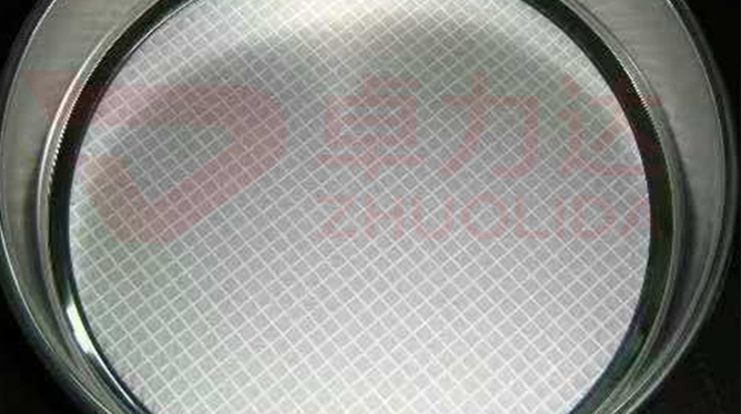
Electroformed microhole mesh wall verticality control governs whether the sidewall stands straight from the front face of a hole to the back. A microhole mesh opens straight-walled cavities in resist by lamination and LDI, then nickel grows up along those resist walls; tilt the wall a little, undercut it a little in development, and the metal copy carries a taper. The aperture tolerance is written as ± 3 μm, but that is only how the mouth is measured; lean the wall and the hole bottom comes out a few microns smaller than the mouth, and fluid flow, paste release and particle screening all run on the narrowest point. The line sections a coupon to measure wall taper, and also takes one aperture reading from each face with a vision system to back out verticality; straight-wall forming simply means those two dimensions sit as close together as possible.
The classic case is development rushed for time: a small foot of undercut eats into the bottom of the resist sidewall, and once the nickel is grown and sectioned the mouth sits inside ± 3 μm while the bottom has necked in, so fines jam midway down the tapered wall during screening and will not flush through. On another lot of atomiser microhole sheets the LDI double-side alignment drifted, front and back openings shifted half a body width apart, the wall became a slanted channel, and the spray cone leaned to one side across the whole sheet. Then there is resist laminated without full contact, a patch lifting locally: after exposure that area of sidewall carries a curve, the flash system scanning flatness sees nothing, and installed flow comes in a notch below the rest of the lot. None of these show up in aperture spot checks; they surface only when flow or release decides performance, by which time a batch is usually already filmed and blanked. Taper is the most deceptive of the lot — measure the front and it looks fine, flip to the back and the hole has necked down to one small end and one large.
Parameter Window
• Aperture tolerance ± 3 μm and position accuracy ± 7 μm, one reading from each face to back out verticality
• Wall taper ≤ 0.5° internal control, sectioned to measure mouth-to-bottom difference
• LDI resolution 8 μm/8 μm, double-side alignment ± 5 μm, maximum substrate 610 × 660 mm
• Stencil thickness 15–200 μm; thick stock means taller resist walls and tighter undercut allowance
• Current density 1–4 A/dm²; deposit too fast and nodules pile at the mouth and shift the taper
• Minimum aperture ≥ 25 μm, web ≥ 50 μm, aperture rib line width 20 μm
Manufacturing Process (8 Steps)
1. Master data — issue the LDI drawing from the hole array, flag straight-wall and alignment requirements separately for the microhole zone.
2. Substrate cleaning — degrease and make conductive, leave no particle on the board before lamination or the resist lifts.
3. Lamination and LDI — imported LDI exposure at ± 5 μm double-side alignment; resist sidewall verticality is fixed here.
4. Development — lock concentration and time so the foot is not undercut and no residue stays; most of the taper is decided in this step.
5. Electroforming — staged current at 1–4 A/dm², nickel grows along the straight resist wall, the mouth does not seal over first.
6. Demolding — release the whole sheet from a low-stress edge; a slanted wall distorts most easily at lift-off.
7. Inspection — section for taper, vision and flash systems read apertures from both faces, checker scans openings.
8. Framing and packing — AB adhesive frame, tension set in 10–55 N bands before shipping.
Core Advantages
1. Straight-wall forming — electroformed microhole mesh wall verticality control holds taper to ≤ 0.5°, so mouth and bottom dimensions stay matched.
2. Apertures genuinely pass — ± 3 μm is not just a surface figure, the whole wall sits inside tolerance.
3. Steady flow — channels do not neck down, so screening and atomising throughput is even across the sheet.
4. Clean release — straight walls hold no paste and trap no powder, so fine-pitch bridging drops away.
5. Dimension and profile handled apart — apertures belong to the checker, taper to sectioning, so a fault localises to the LDI or development run.
6. Traceable — exposure energy, development time and alignment offset logged per sheet, back to the specific substrate.
Typical Applications
1. Precision screens for semiconductor material grading, where a tapered wall traps powder and shifts the cut size.
2. Microhole meshes for atomising and dispensing, where straight walls set spray cone angle and throughput distribution.
3. Mini LED and BGA fine-pitch printing stencils, where a leaning wall makes paste release swing high and low.
4. Thin parts such as optical apertures and encoder discs, where 20 μm ribs need straight walls to avoid blocking light.
5. Filter-membrane support meshes and micro-reaction channel plates, where aperture must stay constant through the depth.
6. Large-format photovoltaic grids, where uneven exposure energy along the long edge drifts taper at both ends first.
Design and Selection Notes
1. Watch lamination contact first; one speck of dust on the board is one curved wall, and no exposure accuracy brings it back.
2. Develop short rather than rushed; a few tenths of a micron of undercut at the foot copies into the nickel as a necked mouth.
3. Recheck double-side alignment at ± 5 μm each lot; half a body width of offset turns the wall into a slanted channel.
4. Do not push current density to the ceiling; a mouth that thickens first seals the lower wall into a taper.
5. Give thick stock its own development allowance by resist wall height; 15–200 μm cannot run on one set of parameters end to end.
6. Set a separate sectioning station for taper recheck; a flat-bed checker cannot read the hole-bottom dimension.
7. Keep the release direction clear of dense microhole zones; a slanted wall is most easily pulled crooked at lift-off.
Laid out, electroformed microhole mesh wall verticality control sits less in the electroforming tank than in the two steps that stand the resist wall straight, exposure and development: how well the film contacts, whether LDI alignment drifted, how much development undercut there is — all copy into nickel as the few microns of difference between mouth and bottom. Measure ± 3 μm aperture accuracy on the front face alone and the taper is simply hidden under a passing report. One atomiser sheet sectioned with edge-zone taper nearly half a degree over the centre, traced to a laminator roller whose pressure was not even across the width. What is hard on the line is not turning out one straight-walled sheet now and then, but holding taper steady at ≤ 0.5° across hundreds of thousands of holes on one substrate and several consecutive lots, so fluid performance matches the drawing. For orders with a hard wall-profile requirement, fix exposure energy, development time, alignment offset and the current density curve into the process card at sampling stage and run to that card in production; it is far cheaper than endlessly retuning the flow bench and release end. On paper electroformed microhole mesh wall verticality control is one taper figure; on the line it is that wall in the section, almost dead straight from front to back.
Contact:赖先生
Phone:+86 18938693450
Tel:0755-2708-8292
Email:yw9@zldsmt.com
Add:深圳市宝安区福永镇新和村福园一路华发工业园A3栋
 Zhuolida