Welcome: Shenzhen Zhuolida Electronics Co.TD
Language:
 ∷

∷
∷
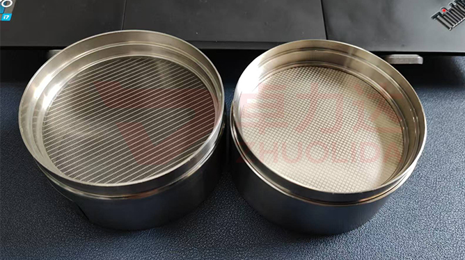
The electroformed mask conductive layer preparation control governs how a continuous, thin enough, just-adherent conductive seed layer is laid on non-conductive substrates such as glass, silicon and ceramics, so nickel starts plating across the whole plate at once and grows to an even thickness. The mask base itself does not conduct; strike plating depends entirely on this seed layer for current. One break in it leaves one patch unplated, a layer too thick or too tightly bonded will not release later, and adhesion too loose makes the nickel blister and lift halfway through deposition. Unlike stencils and screens built on stainless substrates, a mask often uses the substrate as a temporary carrier, so pattern accuracy hangs entirely on seed-layer continuity and evenness — whether ±5 μm double-side alignment and 8 μm/8 μm LDI resolution hold is largely decided in those first minutes of strike plating.
Three failures on the line all sit around strike plating. One is local skip plating: the seed layer breaks at hole zones, plate edges or spots left dirty by pre-treatment, current cannot pass, nickel simply does not grow, the developed pattern loses a corner and a flash gauge finds the opening out of agreement with the design. Two is uneven whole-plate thickness: field lines crowd at the rim and thin out at the centre, so without staging the 1–4 A/dm² current density the deposit ends up thick at the edge and thin in the middle; once the same-plate spread exceeds the ±3 μm internal limit, the thin zones curl first when low-temperature anneal releases stress. Three is blistering and chipped edges: with the adhesion window unfixed, nickel bulges up from the rim mid-run, or lifting the sheet tears the pattern and chips the brittle substrate edge. None of these can be repaired by exposure; what the electroformed mask conductive layer preparation control guards is the interface account from pre-treatment to strike plating.
Parameter Window
• Strike current density staged 1–4 A/dm², the first band held low so the seed layer fills out before stepping up to deposition.
• Maximum substrate 610×660 mm, seed-layer sheet resistance sampled per plate, plates out of band never entering the bath.
• Mask thickness banded 15–200 μm, whole-plate thickness spread held to ±3 μm internally, edge and centre sampled separately.
• Double-side alignment ±5 μm, LDI resolution 8 μm/8 μm, pattern coordinates re-measured once before and once after strike plating.
• Nickel-cobalt alloy hardness 450–550 Hv, wall roughness ≤0.01 μm, hardness weighed together with internal stress.
• Adhesion verified per lot, low-temperature anneal temperature and soak time fixed, not adjusted on the fly.
Manufacturing Process (8 Steps)
1. Substrate pre-treatment — clean, degrease and dry the glass or silicon, leave no dust on the surface, measure flatness first.
2. Conductive treatment — deposit the conductive seed layer, sample sheet resistance per plate, accept only when edges and centre are both covered.
3. Lamination and exposure — write the pattern by LDI after lamination at 8 μm/8 μm resolution, fixing the ±5 μm double-side datum.
4. Development — develop the resist pattern, flush fine ribs and micro-hole zones clean, confirm the seed layer is not masked by resist residue.
5. Strike plating — hold the first 1–4 A/dm² band low, start the whole plate together, watch for any skip-plating spot.
6. Electroforming — step the current up to grow 15–200 μm, holding edge-to-centre spread within ±3 μm as it deposits.
7. Lift-off and anneal — lift the nickel mask off in one sheet from a low-stress corner, then low-temperature anneal to relieve stress.
8. Recheck — vision and flash gauges scan pattern coordinates, openings and flatness, and issue the inspection card with the goods.
Core Advantages
1. Even strike — the electroformed mask conductive layer preparation control ties seed continuity to the first current band so nickel grows across the plate at once.
2. Even thickness — staged current plus edge-to-centre control holds the same-plate spread to ±3 μm, so anneal brings no curl.
3. No skip plating — sheet resistance sampled first keeps broken-film plates out of the bath, so patterns keep their corners.
4. Accurate pattern — ±5 μm double-side readings agree before and after strike plating, coordinates do not move.
5. Releasable — adhesion window verified per lot, the nickel leaves whole, the substrate stays unchipped and the pattern un-torn.
6. Traceable — sheet resistance, first-band current and anneal temperature logged per plate, anomalies traced to the pre-treatment lot.
Typical Applications
1. Nickel masks for evaporation and sputtering, where whole-plate strike on a non-conductive substrate is the first step.
2. Wafer-level masks and semiconductor substrate pattern parts, ±5 μm double-side alignment resting on a steady seed layer.
3. Mini/Micro LED mass-transfer masks, 610×660 mm large plates needing the same thickness at edge and centre.
4. Optical aperture blades and encoder discs, 20 μm rib width and 50 μm±0.5 μm code tracks vulnerable to skip plating.
5. Precision micro-hole meshes and filtration masks, aperture tolerance ±3 μm hanging on even deposition.
6. Export masks needing RoHS and inspection reports, pre-treatment parameters archived with the shipment.
Design and Selection Notes
1. Fix the substrate material first; glass, silicon and ceramics each need different pre-treatment chemistry and seed thickness.
2. Sample seed-layer sheet resistance per plate and redo any plate whose edges are not covered; strike plating will not repair it.
3. Hold the first current band low to fill out before stepping up, do not hit the 4 A/dm² ceiling the moment the plate enters the bath.
4. Verify the adhesion window per lot; too friendly will not release, too loose lifts mid-run, clamp both ends.
5. Measure edge-to-centre spread as it deposits and adjust current distribution once it passes ±3 μm, do not wait for anneal to find out.
6. Put low-temperature anneal after lift-off; reverse the order and stress will have pulled the pattern out of shape.
7. Log pre-treatment, strike plating and recheck data so a disputed pattern can be traced back to the plate.
Taken apart, the electroformed mask conductive layer preparation control is not about spraying a conductive coating onto the substrate but about whether seed continuity, simultaneous strike, even edge-to-centre thickness and just-right adhesion can all hold at once. Sheet resistance sets whether plating skips, the first current band sets whether the strike starts together, current distribution sets whether thickness is even, and adhesion sets whether the sheet releases; loosen any one and ±5 μm double-side alignment and 8 μm resolution never reach the finished part. What separates capable lines is whether thickness still lines up across a dozen plates from one bath and after a fresh lot of substrates, not whether a single plate can grow nickel at all. For orders with hard figures on mask conductive layer uniformity or electroformed mask strike plating pre-treatment, fix substrate pre-treatment, seed sheet resistance, first-band current and the adhesion window into the process card at sampling stage and run to that card in volume — far cheaper than sorting skip-plated plates one by one.
Contact:赖先生
Phone:+86 18938693450
Tel:0755-2708-8292
Email:yw9@zldsmt.com
Add:深圳市宝安区福永镇新和村福园一路华发工业园A3栋
 Zhuolida
