Welcome: Shenzhen Zhuolida Electronics Co.TD
Language:
 ∷

∷
∷
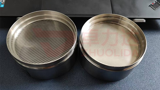
Electroformed micro-structured optical elements are optical parts carrying micron- or even nanometer-scale structures — diffraction gratings, microlens arrays, grating scales — produced by copying those structures onto metal through electroforming. The thinking is entirely different from conventional optical fabrication: grinding and polishing remove material, single-point diamond turning walks a tool one pass at a time, while electroforming grows the master's structure directly into metal. Whatever the master has, the plated metal part has. Because deposition is atomic-level, structural fidelity is high, and one master can be replicated into thousands of identical parts, which suits optical elements that demand tight surface figure, dense micro-structure, and batch consistency.
Optical systems keep shrinking — elements drop from tens of millimeters to a few millimeters while structures become denser, with grating pitches down to sub-micron and hundreds of units packed into one microlens array. Traditional glass molding suffers from mold life and high-temperature creep, and precision falls as volume rises. Single-point diamond turning handles aspheres and freeforms, but dense grating grooves or micro-pillar arrays force the tool to cut one line at a time — slow, costly, and prone to chipping in deep grooves. Glass etching of transmissive structures struggles to balance sidewall verticality and depth uniformity. Electroforming fills this gap: a master is made once by photolithography or etching, and metal deposition reproduces the structure precisely, with surface roughness down to the nanometer range. For reflective metal optics it also brings heat spreading and high-power tolerance, so in infrared and laser scenarios where heat and power are concerns, a metal substrate can beat glass. The real difficulty lies in master preparation and demolding — the finer the structure, the more delicate the master, and uneven demolding tears or distorts it.
Parameter Window
• Structure feature size: 0.5–50 µm, from grating groove width to microlens aperture
• Surface roughness: Ra < 5 nm, meeting visible to near-infrared reflection needs
• Surface figure: PV < λ/4, close to the diffraction limit
• Coating thickness: 0.05–2 mm, chosen by stiffness and heat-spreading needs
• Common materials: electroformed nickel, nickel-cobalt alloy, copper; nickel more wear- and corrosion-resistant
• Replication fidelity: sub-micron, master structure transferred as-is
Manufacturing Process (8 Steps)
1. Master preparation — photolithography, etching, or diamond turning builds the micro-structured master, controlling groove shape and sidewalls.
2. Conductive treatment — non-conductive masters get a thin conductive layer; metal masters are cleaned and activated for uniform strike.
3. Electroforming replication — nickel deposits layer by layer on the master, filling the micro-structure and growing to the required thickness.
4. Demolding — stress and temperature are controlled for slow separation, avoiding tears or figure drift in fine structures.
5. Post-processing — polish away backside allowance and apply reflective or protective coatings as needed.
6. Figure inspection — an interferometer measures figure and roughness against diffraction requirements.
7. Optical performance test — check diffraction efficiency, stray light, and wavefront error, screening out rejects.
8. Cleaning and packaging — clean and vacuum-pack to keep dust from scratching the micro-structure.
Core Advantages
1. High-fidelity replication — atomic-level deposition transfers the master micro-structure as-is, losing no detail.
2. Large-area consistency — one master replicates in batches with very small part-to-part deviation.
3. Metal reflection, high power — metal substrates conduct heat and tolerate high power, fitting lasers and infrared.
4. Reusable master — made once and used long, amortizing per-part cost.
5. Shape freedom — aspheres, freeforms, and variable-pitch arrays form in one shot.
6. Fast iteration — changing the structure only means changing the master, not the whole process.
Typical Applications
• Diffraction gratings — spectrometers and laser splitting, where groove shape sets resolution.
• Microlens arrays — sensing, display, and light-field imaging that boost light collection.
• Diffractive optical elements (DOE) — beam shaping, diffusion, and homogenizing, replacing multi-lens stacks.
• Grating scales — encoder displacement measurement; metal gratings resist wear and contamination.
• Infrared optics — thermal imaging and IR detection; metal mirrors endure high and low temperatures.
• Laser shaping elements — homogenizing and focusing of high-power lasers, where metal substrates take the heat.
Design and Selection Points
1. Match structure feature size to coating thickness; too thin cannot fill deep grooves.
2. Choose master material by volume — silicon or glass for small runs, metal molds for high volume.
3. Calculate thermal stress before demolding; a large expansion mismatch between nickel and master can tear fine structures.
4. Control coating internal stress; excessive stress warps the part and hurts figure accuracy.
5. For figure deviation, apply compensation machining first rather than relying on post-polishing.
6. Select reflective coating by band — gold or aluminum for IR, silver or aluminum plus a protective layer for visible.
7. Inspection must cover figure, roughness, and diffraction efficiency; testing only one can miss defects.
Electroformed micro-structured optical elements have earned their place in precision optics by copying the master's micro-structure one-to-one onto metal, preserving sub-micron detail while producing figure-consistent parts in volume. Against grinding, turning, and glass molding, they strike a balance between dense micro-structure and high volume, and the metal substrate adds heat conduction and high-power tolerance on top. As infrared imaging, laser processing, and optical communication push toward smaller, more integrated optics, electroformed micro-structured optical elements will only find more use. Choosing them means buying a combination of structural fidelity, batch stability, and metal properties — the fundamental difference from conventional optical cold working. As elements get smaller and structures denser, guarding the precision floor at the replication step is often more reliable than fixing later, and better supports the yield and consistency of high-end optical products.
Contact:赖先生
Phone:+86 18938693450
Tel:0755-2708-8292
Email:yw9@zldsmt.com
Add:深圳市宝安区福永镇新和村福园一路华发工业园A3栋
 Zhuolida