Welcome: Shenzhen Zhuolida Electronics Co.TD
Language:
 ∷

∷
∷
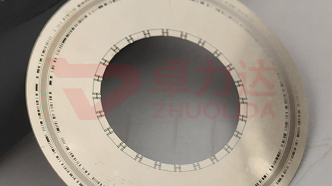
Probe positioning template hole accuracy control is not about how accurately a single hole is made; it is about whether the whole pattern sits where the datum says. A wafer test fixture finds its coordinates from datum holes and a datum edge on the template, then drives each probe down onto a pad from that frame. However tidy the array pitch is, a few microns of overall shift relative to the datum means every probe lands off at assembly. So this process puts datum holes and array into one coordinate system at the artwork stage — one exposure, one deposition, one re-measurement, no re-clamping in between. Position accuracy of ±7 μm is the delivery figure, but it has to be read against the datum; clean pitch between holes says nothing about whether the fixture will work.
The most common floor mistake is doing it in two setups. Machine the datum holes first, add the array later, and one slip of the fixture shifts the whole array relative to the datum; probes land on pad edges or into empty space at assembly, while the array pitch checks out perfectly on its own. The second is aligning on single-side marks only, so the ±5 μm double-side margin gets eaten by two stacked errors and the outer rows touch the limit first. Stress release after release adds its own shift — the pattern translates a little, and a cross-section re-measurement is where the datum-to-array distance turns out changed. Then there is inspecting the array but not the datum: every hole passes on the report, yet the whole set sits to one side when the fixture is mounted. The shared feature of all these is that the holes are right but the coordinate frame is not, and that frame is exactly what probe positioning template hole accuracy control has to hold.
Parameter Window
• Position accuracy ±7 μm; the datum-to-array offset and the pitch between holes are controlled as separate items.
• Minimum aperture ≥25 μm, pitch ≥120 μm, web ≥50 μm; dense arrays are the most sensitive to accumulated deviation.
• Aperture accuracy ±3 μm; probe clearance is held by aperture and position together.
• Lamination LDI resolves 8 μm/8 μm with ±5 μm double-side alignment; alignment error passes straight into the positioning datum.
• Stencil thickness 15–200 μm; wall verticality on a thick template affects how the probe descends.
• Bath current density 1–4 A/dm²; re-measure the datum-to-array offset after stress release.
Manufacturing Process (8 Steps)
1. Datum design — fix datum holes and datum edge first, then lay out the probe array, avoiding a second setup.
2. Pre-treatment — clean and conductivise the substrate, passivate the mandrel face for low adhesion.
3. Lamination and LDI — one imported LDI exposure carries datum and array together at 8 μm/8 μm resolution, ±5 μm double-side alignment.
4. Development — open every hole shape, no scum at the base, no resist narrowing the datum holes.
5. Deposition — staged 1–4 A/dm² control, low internal stress, less overall translation after release.
6. Release and anneal — peel the whole sheet from a low-stress corner, low-temperature anneal sets the shape.
7. Position re-measurement — vision system, flash measurement and automatic checker scan all holes in the datum coordinate frame.
8. Fixture trial fit — mount on the wafer test fixture, confirm probe-to-pad alignment before delivery.
Core Advantages
1. One coordinate frame — datum and array formed in a single exposure, with probe positioning template hole accuracy control set from the start and no relative shift from a second setup.
2. Probes land true — ±7 μm judged against the datum, so the fixture aligns once without shimming on site.
3. Outer rows clear — the double-side alignment margin serves the whole sheet, so edge rows do not fail first.
4. Stress contained — low-stress deposition plus anneal keeps datum-to-array from translating after release.
5. Reviewable — each sheet carries a full-sheet position map in the datum frame the fixture maker can use directly.
6. Fast changeover — a new array only means new artwork data, the datum system carries over and trial fit stays short.
Typical Applications
1. Probe positioning templates for wafer test fixtures, where a shifted datum sends every probe off its pad.
2. Probe cards and vertical probe socket parts, where position and aperture together set insertion clearance.
3. Wafer-level ball-placement masks, where array and alignment marks are copied on one master to avoid a second alignment.
4. BGA and Mini LED fine-pitch printing stencils, whose datum edge must also be formed with the openings in one pass.
5. Encoder discs and aperture blades, where track position relative to the centre datum matters more than line width.
6. Multi-sheet assemblies of semiconductor grading screens, where a shared datum is what makes a continuous screening surface.
Design and Selection Notes
1. Lock datum holes and datum edge at the artwork stage, do not drill locating holes into a finished part.
2. Datum and array must share one LDI exposure; two passes are an invitation to shift.
3. Issue the report in the datum coordinate frame; passing pitch does not mean passing position.
4. Hold current density in one segment of 1–4 A/dm²; a change in stress drifts datum-to-array with it.
5. The ±5 μm double-side figure belongs to exposure; post-release datum re-measurement is the delivery figure.
6. Watch wall verticality on thick templates, probe descent depends on more than hole position.
7. Run one fixture trial fit at sampling stage and write the result into the process card before volume.
Put probe positioning template hole accuracy control back on the whole line and it governs a coordinate relationship, not the size of a row of holes. One-master datum gives 'no re-clamping', double-side alignment gives 'two layers not stacked', datum-frame re-measurement gives 'the fixture mounts'; only then is ±7 μm more than a number on a report. What separates capable lines is rarely whether one hole can be placed, but whether the farthest row of the array from the datum still lands inside the window. For orders specifying wafer test template datum, fix the datum scheme, exposure method and re-measurement frame into the process card at sampling stage, then scan full sheets and trial fit to that card in production, far cheaper than shimming the fixture into alignment on the assembly floor. That is where probe positioning template hole accuracy control earns its keep: spelling out exactly what the accuracy is relative to.
Contact:赖先生
Phone:+86 18938693450
Tel:0755-2708-8292
Email:yw9@zldsmt.com
Add:深圳市宝安区福永镇新和村福园一路华发工业园A3栋
 Zhuolida
