Welcome: Shenzhen Zhuolida Electronics Co.TD
Language:
 ∷

∷
∷
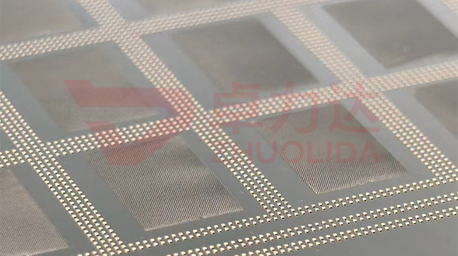
A stencil carries a million apertures. Dimensions measured, positions aligned, and still the print comes out short on solder — the fault usually sits in a geometric quantity that never makes it onto the drawing: the aperture area ratio. It is the bottom area of an aperture divided by the four wall side areas, (L×W)/[2(L+W)×T] for a rectangle and D/4T for a round hole, and the line treats 0.66 as the cutoff for clean release. Precision electroformed stencil aperture area ratio control governs how this ratio lands inside the design window across 15–200μm thickness: with pad width fixed, every step up in thickness drags the ratio down, and once it slips past 0.66 the paste no longer drops as one block.
The most common trap on the floor is blaming every solder shortage on the paste or the squeegee. One batch of Mini LED fine-pitch stencils measured inside ±3μm on every aperture, yet SPI kept reporting falling deposits on 01005 pads; a wipe brought the volume back, and side lighting showed a thin film of paste clinging inside the openings. Another net from the same lot bridged on the large QFN pad while starving the 01005s — the 40μm thickness had not been trimmed to the aperture width and the ratio had sunk just past 0.6. More subtle still: a run of 25μm thin stencils was calculated to be fine, but developer undercut had eaten the aperture mouths wider, leaving real walls thicker than designed; transfer efficiency fell to about 70 percent and the stencil needed constant wiping long before 15000 prints. Precision electroformed stencil aperture area ratio control is hard because the ratio never appears in the dimensional report: the flat inspection machine scans aperture outlines, it cannot compute a value that includes wall thickness, and by the time a shortage shows up a whole carrier panel is already scrap.
Parameter Window
• Area ratio AR≥0.66 as the release boundary, held above 0.70 internally for fine pitch
• Stencil thickness 15–200μm; for the same aperture, every 10μm added pulls the ratio down
• Minimum aperture ≥25μm, pitch ≥120μm, web ≥50μm; the ratio bottoms out first as openings narrow
• Aperture accuracy ±3μm and position accuracy ±7μm, tracked separately from the area ratio
• Wall roughness ≤0.01μm; a smooth wall lets the 0.66 boundary relax one notch
• Tension 10–55N (±1N internal); recheck ratio decay against a 15000-print life
Manufacturing Process (8 Steps)
1. Data and drawing — compute the area ratio aperture by aperture from the pad map, flag anything below 0.66 and change the thickness class first.
2. Pretreatment — clean and conductivize the base, passivate the mandrel face so plating starts evenly without pinholes.
3. Lamination and LDI — 8μm/8μm resolution, double-side alignment ±5μm; the aperture geometry is fixed here.
4. Developing — control developer concentration and time, leave no residue at the bottom and no undercut on the sidewalls, then recheck the ratio against the as-built wall thickness.
5. Electroforming — current density 1–4A/dm² in staged control, stop the moment target thickness is reached; overgrowth pushes the ratio down.
6. Demolding — peel the whole sheet from a low-stress corner so aperture mouths do not collapse and the area stays true.
7. Inspection — the checker scans apertures, an imager and a flash gauge verify positions, and the ratio is computed from measured thickness.
8. Mounting and packing — aluminum frame bonded with AB adhesive, tension set in 10–55N steps before shipment.
Core Advantages
1. Stable transfer — holding precision electroformed stencil aperture area ratio control above 0.66 suppresses shortage and bridging together.
2. Clean release — with enough ratio, paste drops as one block and leaves no tails on the walls.
3. No need to lean on thin stock — pick a class across 15–200μm by ratio instead of thinning everything to force release.
4. Size and geometry managed apart — ±3μm aperture accuracy goes to the checker, the ratio to the process card, and anomalies trace back to a thickness class.
5. Honest life — with ratio margin built in, decay toward 15000 prints is slower.
6. Traceable — every sheet records thickness, aperture size and computed ratio, traceable to a specific bath run.
Typical Applications
1. Mini LED and 01005 fine-pitch printing stencils, where small openings hit the ratio floor first.
2. 4–12 inch WLP ball-drop templates, where a million openings must transfer the same volume.
3. ABF substrate Ball and Flux plates, the Ball side being fussier about the ratio.
4. Precision sieves for semiconductor material classification, whose micro-hole geometry obeys the same ratio constraint.
5. Composite plates with Post or local thickening, where the step changes thickness and the ratio must be checked on its own.
6. Large-format grids such as photovoltaic stencils, where whole-sheet thickness uniformity holds the ratio consistent.
Design and Selection Notes
1. Back out thickness from pad size first — once aperture width is fixed, the 0.66 boundary caps how thick the sheet can be.
2. Do not watch aperture accuracy alone — ±3μm can pass while the ratio fails, and the press still shorts solder.
3. Read wall roughness alongside it — Ra≤0.01μm widens the usable boundary by a notch.
4. Do not rush developing — a few tenths of a micron of undercut changes the real aperture area.
5. Set up a separate station for stencil aperture area ratio inspection; a checker scanning outlines cannot compute a value that involves wall thickness.
6. Set tension in 10–55N steps and never mix classes in one lot, or transfer efficiency will not line up.
7. On thickened plates, check the ratio at the thickness transition between the Post region and the thin web separately.
Break precision electroformed stencil aperture area ratio control apart and it owns no single step: LDI and developing fix the aperture outline, the bath decides which thickness class to stop at, and the few seconds of demolding decide whether the mouths collapse. Pretreatment, exposure, deposition and peeling each guard one stretch, and if any of them loosens, the 0.66 line will not hold. The ratio drifts with thickness lot and develop time, so it has to be sampled per bath. What is hard is not producing one passing sheet by chance, but keeping a dozen sheets from the same bath and several consecutive lots sitting in the same ratio class — only then does ±3μm aperture accuracy mean anything. For orders with a hard requirement on fine-pitch transfer, fix aperture size, target thickness and develop time in the process card at the sampling stage and run production to that card; it is far cheaper than endlessly tuning demold speed, swapping paste and wiping the stencil at the printer.
Contact:赖先生
Phone:+86 18938693450
Tel:0755-2708-8292
Email:yw9@zldsmt.com
Add:深圳市宝安区福永镇新和村福园一路华发工业园A3栋
 Zhuolida
