Welcome: Shenzhen Zhuolida Electronics Co.TD
Language:
 ∷

∷
∷
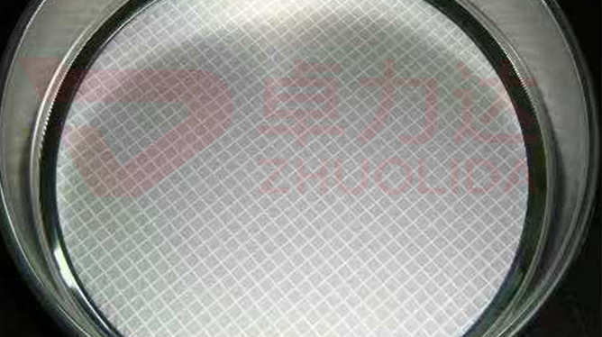
Lay a 20–200 μm nickel screen under a vision measuring system and two things get read: how large each hole is, and where it landed. Electroformed screen aperture accuracy control is the discipline of holding aperture size to ±0.003 mm and hole-centre position to ±0.005 mm, with data to back every sheet. It is not a single step but an acceptance standard spanning master artwork, LDI exposure, electrodeposition and post-release re-measurement. Semiconductor material grading, lithium-battery separator screening and PCB processing screens are all specified in microns; once ±0.003 mm or ±0.005 mm is exceeded, a bright screen is still scrap.
Deviation does not appear at measurement — it accumulates. If the master artwork leaves no allowance for development undercut, the developed opening ends up a few microns under design. LDI resolution of 8 μm/8 μm describes line-width resolving power and ±5 μm double-side alignment describes front-to-back registration; neither equals finished hole position. In the bath, extra brightener refines the grain and pushes hardness toward 450–550 Hv while internal stress rises with it; lift current density from 1 to 4 A/dm² and the deposition rate spread between the edge and centre of a 610×660 mm panel opens up, which is where thickness error of ±0.005 mm comes from. Release removes the constraint, stress lets go, the thin foil bows slightly and hole positions drift. That is why the line's real headache is a post-release re-measure failure — exposure can be perfectly aligned and the job still lost to unmanaged stress. Holding ±0.003 mm means logging master data, exposure registration, deposition stress and release springback separately, then reading every sheet back on a vision system or flash measurement.
Parameter Window
• Screen thickness 20–200 μm; below 30 μm hole position is more sensitive to stress springback
• Aperture size accuracy ±0.003 mm, delivered against post-release vision measurement
• Hole-centre position deviation within ±0.005 mm, sampled by zone across the full 610×660 mm panel
• Thickness error ±0.005 mm and roundness tolerance ±0.002 mm logged for the same lot
• Minimum corner radius 0.01, nickel alloy hardness 450–550 Hv, hardness coupled with stress
• LDI resolution 8 μm/8 μm, double-side alignment ±5 μm, RoHS compliant
Manufacturing Process (8 Steps)
1. Artwork preparation — derive the aperture pattern from the target particle size, allowing for development undercut and electroforming shrinkage.
2. Pre-treatment — substrate cleaning and conductive coating, with low-adhesion passivation of the mandrel face for one-piece release.
3. Lamination and LDI — imported LDI exposure at 8 μm/8 μm resolution, ±5 μm double-side alignment, substrates up to 610×660 mm.
4. Development and electroforming — staged control of current density and temperature after development keeps stress down as the layer grows.
5. Demolding — start from a low-stress corner, control angle and speed for one-piece release, support thin zones before lifting.
6. Stress relief — low-temperature anneal removes residual stress so springback does not shift hole positions.
7. Inspection — vision system and flash measurement read every aperture and position; hardness tester logs the 450–550 Hv state.
8. Cutting and packing — cut to frame size with a per-sheet measurement report and RoHS documents.
Core Advantages
1. Repeatable apertures — ±0.003 mm locked by master compensation and development control, not by sorting good sheets.
2. Position stays put — post-release re-measurement is the standard; deposition stress and low-temperature anneal minimise springback.
3. Panel-wide consistency — several sheets from one 610×660 mm panel share a bath, with edge-to-centre thickness spread inside the control line.
4. Stable roundness — ±0.002 mm roundness and the 0.01 minimum corner radius are formed once at the mandrel stage.
5. Traceable data — aperture, position, thickness and hardness logged per sheet; anomalies trace back to bath run and exposure number.
6. Compliance ready — the nickel alloy meets RoHS, so medical and food filtration orders need no separate material statement.
Typical Applications
• Semiconductor material grading, holding powder to a narrow size band with ±0.003 mm apertures.
• Lithium-battery separator coating and screening, where ±0.005 mm position keeps the hole array even.
• PCB drilling and forming screens, sensitive to wall integrity in thin-web zones.
• Electronic-grade paste filtration, where 450–550 Hv hardness balances wear life and cleanability.
• Fine chemical filtration, where ±0.002 mm roundness stabilises the flow coefficient.
• Pharmaceutical screening and test meshes, delivered with RoHS and a per-sheet report.
Design and Selection Notes
1. Fix the thickness band first. Screens of 20–30 μm should carry support during release rather than be pulled bare.
2. State whether aperture tolerance refers to exposure or post-release; ±0.003 mm means the latter.
3. Verify position deviation by zone across the panel; logging the 610×660 mm edge zones separately is safer.
4. Do not chase hardness. 450–550 Hv is sufficient; pushing higher drags hole positions off with internal stress.
5. Leave development-undercut allowance in the master artwork and write ±0.002 mm roundness into the drawing for round holes.
6. The ±5 μm double-side figure belongs to exposure; post-release position re-measurement is the delivery figure.
7. For screens with local thickening or shaped openings, choose a release direction that avoids the step root of the thickened zone.
Seen on its own, electroformed screen aperture accuracy control governs not 'making the holes' but 'still being able to measure them afterwards'. Master compensation aligns the design value, LDI registration keeps front and back consistent, and low-stress deposition with controlled release stops the screen springing out of shape — miss any one and neither ±0.003 mm aperture tolerance nor ±0.005 mm position deviation reaches the delivery note. That is the part of electroformed screen aperture accuracy control most often misread: many treat it as one inspection, when it is really a joint audit of exposure, deposition and release. What separates capable lines is not whether a 20–200 μm screen can be plated, but whether a dozen sheets from one 610×660 mm panel all finish on the same set of numbers. For semiconductor grading or lithium-battery separator orders with tight size bands, fix the master compensation, development-undercut factor, anneal temperature and release start point into the process card at sampling stage and run to it. Precision screen aperture tolerance control and electroformed screen position deviation control go by different names, yet on the shop floor both come down to one thing: making electroformed screen aperture accuracy control a report every sheet can be signed against.
Contact:赖先生
Phone:+86 18938693450
Tel:0755-2708-8292
Email:yw9@zldsmt.com
Add:深圳市宝安区福永镇新和村福园一路华发工业园A3栋
 Zhuolida