Welcome: Shenzhen Zhuolida Electronics Co.TD
Language:
 ∷

∷
∷
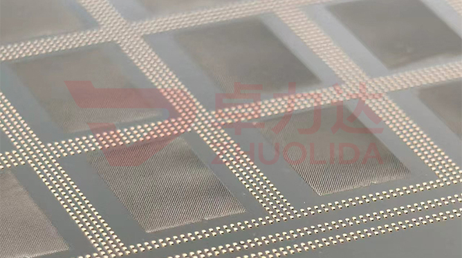
A 25 μm ball-placement stencil has grown its several hundred thousand apertures. Position accuracy of ±7 μm and aperture accuracy of ±3 μm have both been measured. The last move is to lift the nickel off the mandrel. Lift it cleanly and everything upstream counts; tear one edge, or let the foil bow in the middle and keep a permanent set, and the sheet is scrap. Precision electroformed stencil demolding governs exactly this passage from "still stuck to the tool" to "a free-standing part". Unlike deposition, there is no half hour of parameter tuning here — it takes a few seconds and depends entirely on conditions laid down earlier.
The difficulty is that stress accumulates. Push the brightener concentration up and the grain refines and hardness climbs, but so does internal stress. Raise current density from 1 to 4 A/dm² and deposition speeds up while the thickness spread between edge and centre widens. Let bath temperature wander two or three degrees and stress is no longer uniform across one sheet. None of this shows during deposition: the foil is still clamped to a rigid substrate. Release it and the constraint disappears; stress lets go at once, the thin foil curls or warps, and aperture positions drift with it. When a post-release re-measure fails on position, LDI alignment is rarely the culprit — uncontrolled stress usually is. The mandrel side matters just as much. Make the conductive layer too friendly and the nickel bites hard, so release force tears the edge; make it too slippery and the deposit may lift locally mid-run. That adhesion window is narrower than most people expect.
Parameter Window
• Stencil thickness: 15–200 μm; release gets sharply harder below 30 μm
• Minimum aperture ≥25 μm, pitch ≥120 μm, web ≥50 μm
• Position accuracy ±7 μm, aperture accuracy ±3 μm, re-checked after release
• Stencil tension 10–55 N in graded bands; ±1 N as the internal control line
• Aperture wall roughness ≤0.01 μm; low-adhesion nickel surface forms here
• Nickel alloy hardness 450–550 Hv; hardness and internal stress must be weighed together
Manufacturing Process (8 Steps)
1. Artwork preparation — master data for the aperture pattern, from hundreds of thousands to millions of openings.
2. Pre-treatment — substrate cleaning and conductive coating, with low-adhesion passivation of the mandrel face.
3. Lamination and LDI — imported LDI exposure at 8 μm/8 μm resolution, ±5 μm double-side alignment, substrates up to 610×660 mm.
4. Development and electroforming — staged control of current density and temperature keeps stress down as the layer grows.
5. Demolding — start from a low-stress corner, control angle and speed for one-piece release, support thin zones before lifting.
6. Stress relief — low-temperature anneal removes residual stress so dimensions stay put during framing.
7. Inspection — automatic stencil checker for openings and position, vision and flash measurement for confirmation, hardness tester for deposit state.
8. Framing and packing — aluminium frame bonded with AB adhesive, tension set to band before shipping.
Core Advantages
1. One-piece release — adhesion and stress controlled together, no torn edges or nickel residue on thin foils.
2. Dimensional stability — pre- and post-release position readings agree, so no compensation allowance is needed.
3. Intact aperture walls — tapered walls and smooth surfaces survive release undamaged, helping flux and solder paste transfer.
4. Batch consistency — multiple sheets from one 610×660 mm panel share release conditions, narrowing lot-to-lot spread.
5. Traceable yield — release start point, tension and hardness logged per sheet; anomalies trace back to the bath run.
6. Service life secured — stress-relieved sheets drift less after framing, reaching 15,000 prints on chip-substrate work.
Typical Applications
• 4–12 inch WLP ball placement, where millions of openings rule out laser machining.
• ABF substrate ball-placement masks, with Ball and Flux stencils tensioned in separate bands.
• BGA and Mini LED printing stencils, sensitive to wall integrity at fine pitch.
• Large-format photovoltaic grid stencils, where flatness after release is critical.
• Precision screens for semiconductor material grading, equally vulnerable to release distortion.
• Composite stencils with post height or local thickening, harder to demold than uniform sheets.
Design and Selection Notes
1. Fix the thickness band first. Foils of 15–30 μm should carry temporary support during release rather than be pulled bare.
2. Do not chase hardness. 450–550 Hv is sufficient; pushing higher drags internal stress up with it.
3. In dense aperture fields, lower the strike current density so edge effects do not widen the thickness spread.
4. Verify mandrel passivation thickness per lot: too thin risks biting, too thick risks mid-run lifting.
5. The ±5 μm double-side figure belongs to exposure; post-release position re-measurement is the delivery figure.
6. Set tension within one of the 10–55 N bands and never mix bands in a lot, or paste release behaviour will differ.
7. Where posts or local thickening exist, choose a release direction that avoids the step root of the thickened zone.
Seen on its own, precision electroformed stencil demolding is less a standalone step than an audit of pre-treatment, exposure and deposition. A low-adhesion mandrel makes the sheet liftable; low-stress deposition keeps it flat once lifted; controlled peel speed keeps it intact during the lift. Miss any one of the three and ±3 μm aperture accuracy will not hold. What separates capable lines from the rest is rarely whether a stencil can be made at all, but whether a dozen sheets from one bath all come off in the same state. For orders that specify ball-placement stencil stress control, fix the release start point, anneal temperature and tension band into the process card at sampling stage, then run to that card in production — far cheaper than reworking sheets afterwards. That is where precision electroformed stencil demolding earns its keep: turning a few seconds at the end into a repeatable, traceable set of parameters.
Contact:赖先生
Phone:+86 18938693450
Tel:0755-2708-8292
Email:yw9@zldsmt.com
Add:深圳市宝安区福永镇新和村福园一路华发工业园A3栋
 Zhuolida