Welcome: Shenzhen Zhuolida Electronics Co.TD
Language:
 ∷

∷
∷
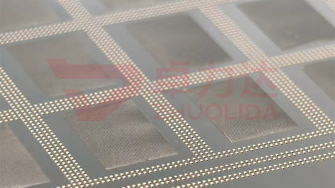
Whether paste releases well used to be a matter of the operator's feel at the moment of demolding; as data it is simply a ratio — transfer efficiency TE, the paste volume printed on the pad divided by the aperture volume itself. Below about 80 percent TE, fine pitch starts to starve; if TE slides down over a dozen prints on one stencil, the walls are holding paste. Electroformed stencil solder paste release verification turns this into a reproducible criterion: measure deposited volume by SPI or weighing after printing, watch the decay curve over consecutive prints, and inspect wall residue under a microscope after demounting — all three together count as a pass. It relates to aperture accuracy ±3μm and wall roughness ≤0.01μm, yet neither of those can stand in for it.
The usual case is a stencil that looks fine while the print data drifts. One lot of QFN fine-pitch stencils dropped from full deposit to 75 percent by the fifth board on SPI, recovered after a wipe, and showed a film of paste on the aperture sidewalls under side lighting; two sheets from the same bath both measured within ±3μm / ±7μm on size and position, yet one demolded cleanly and the other left paste after three prints — the difference was only an invisible nodule layer on the walls. A paste lot change made it worse: 01005 pads bridged, cross-sections showed unreleased paste packed at the aperture bottom, and aperture remeasurement still passed. None of this appears in a flat checker's report, and by the time SPI alarms a batch of substrates is already scrap. Electroformed stencil solder paste release verification gets its own station because dimensional inspection cannot read what happens in those few seconds of demolding.
Parameter Window
• Transfer efficiency TE≥80% as the acceptance line, held above 85% internally for fine pitch
• TE scatter within ±5% over 20 consecutive prints; decay under 10% across a 15000-print life
• Minimum aperture ≥25μm, pitch ≥120μm, web ≥50μm; smaller openings release harder
• Aperture accuracy ±3μm, position accuracy ±7μm, remeasured separately from release volume
• Wall roughness ≤0.01μm; the smoother the wall, the less paste remains
• Stencil thickness 15–200μm and tension 10–55N (±1N internal) set the demold speed window together
Manufacturing Process (8 Steps)
1. Data and drawing — define apertures from the pad map, mark release verification points in fine-pitch zones.
2. Pretreatment — clean and conductivize the base, passivate the mandrel to keep starting nodules off the wall.
3. Lamination and LDI — 8μm/8μm resolution, double-side alignment ±5μm; aperture sidewalls take shape here.
4. Developing — control concentration and time, no residue at the bottom and no starting points for paste to grab on the walls.
5. Electroforming — current density 1–4A/dm² in stages, suppress grain coarsening and nodules.
6. Demolding — peel the whole sheet from a low-stress corner, no torn mouths or collapsed edges.
7. Inspection — checker measures apertures, imager and flash gauge verify positions, SPI samples transfer volume.
8. Mounting and packing — aluminum frame bonded with AB adhesive, tension set in 10–55N steps before shipment.
Core Advantages
1. Reproducible criterion — electroformed stencil solder paste release verification speaks in TE curves, not operator feel.
2. Early lot screening — pull paste-grabbing sheets at the sampling stage instead of finding out on the line.
3. Size and release managed apart — ±3μm goes to the checker, TE to SPI, anomalies traced to a bath run.
4. Controlled wall — pressing roughness to Ra≤0.01μm cuts wall residue noticeably.
5. Honest life — a flat release curve means fewer wipes as prints approach 15000.
6. Traceable — each sheet keeps its TE curve, thickness and tension class for bath-lot lookup.
Typical Applications
1. Mini LED and 01005 fine-pitch printing stencils, where small openings hold paste most easily.
2. 4–12 inch WLP ball-drop templates, where a million openings must transfer the same volume.
3. ABF substrate Ball and Flux plates, the Ball side fussiest about demolding.
4. Precision sieves for semiconductor material classification, where micro-hole release also depends on wall condition.
5. Composite plates with Post or local thickening, where steps tend to pool paste.
6. Large-format grids such as photovoltaic stencils, where whole-sheet release consistency drags yield.
Design and Selection Notes
1. Build a baseline with SPI first — 20 consecutive prints on one aperture, then talk acceptance once TE distribution is stable.
2. Do not watch aperture accuracy alone — ±3μm can pass while TE drifts, and the sheet is still scrap.
3. Read wall roughness alongside it — Ra≤0.01μm is the premise for fine-pitch demolding.
4. Set demold speed by thickness class — slow for 15–30μm thin stock, never yank it.
5. Set up a separate station for stencil paste release rate test; a flat checker cannot read residual paste volume.
6. Set tension in 10–55N steps and never mix classes in one lot, or TE curves will not line up.
7. Re-run verification on a paste lot change — viscosity moves, so the criterion has to be recalibrated.
Laid out, electroformed stencil solder paste release verification spans both sides of shipment: LDI and developing shape the resist sidewalls, the bath decides how grains grow, the few seconds of demolding decide whether walls get pulled into paste-grabbing starting points, and at the customer's line demold speed and wipe intervals amplify or erase all of it. Aperture ±3μm or wall Ra alone explains only half. What is hard is not certifying one sample with a pretty TE curve, but keeping a dozen sheets from one bath and several consecutive lots inside the same TE band — only then does the 15000-print life claim stand. For orders with a hard demolding requirement, fix current density, develop time and SPI sampling points in the process card at the sampling stage and sample production to it; that is cheaper than endlessly tuning speed, swapping paste and adding wipes at the printer. On paper electroformed stencil solder paste release verification is a set of curves; on the line it is every sheet releasing paste as crisply on print one as on print ten thousand.
Contact:赖先生
Phone:+86 18938693450
Tel:0755-2708-8292
Email:yw9@zldsmt.com
Add:深圳市宝安区福永镇新和村福园一路华发工业园A3栋
 Zhuolida
